- 您現(xiàn)在的位置:買(mǎi)賣(mài)IC網(wǎng) > PDF目錄9449 > NBVSPA017LNHTAG (ON Semiconductor)IC VCXO LVDS 156.25MHZ 6CLCC PDF資料下載
參數(shù)資料
| 型號(hào): | NBVSPA017LNHTAG |
| 廠商: | ON Semiconductor |
| 文件頁(yè)數(shù): | 1/8頁(yè) |
| 文件大小: | 0K |
| 描述: | IC VCXO LVDS 156.25MHZ 6CLCC |
| 標(biāo)準(zhǔn)包裝: | 100 |
| 系列: | PureEdge™ |
| 類型: | VCXO |
| 頻率: | 156.25MHz |
| 電源電壓: | 2.97 V ~ 3.63 V |
| 電流 - 電源: | 75mA |
| 工作溫度: | -40°C ~ 85°C |
| 封裝/外殼: | 6-CLCC |
| 包裝: | 帶卷 (TR) |
| 供應(yīng)商設(shè)備封裝: | 6-CLCC(7x5) |
| 安裝類型: | 表面貼裝 |
Semiconductor Components Industries, LLC, 2010
December, 2010 Rev. 1
1
Publication Order Number:
NBVSPA015/D
NBVSPA015 Series
3.3 V, LVDS
Voltage-Controlled Clock
Oscillator (VCXO)
PureEdge
t Product Series
The NBVSPXXXX voltagecontrolled crystal oscillator (VCXO)
devices are designed to meet today’s requirements for 3.3 V LVDS
clock generation applications. These devices use a high Q
fundamental mode crystal and Phase Locked Loop (PLL) multiplier to
provide a wide range of frequencies from 60 MHz to 700 MHz
(factory configurable per user specifications) with a pullable range of
±100 ppm and a frequency stability of ±50 ppm. The siliconbased
PureEdge
t products design provides users with exceptional
frequency stability and reliability. They produce an ultra low jitter and
phase noise LVDS differential output.
The NBVSPXXXX series devices are a member of ON
Semiconductor’s PureEdge
t clock family that provides accurate and
precision clock generation solutions.
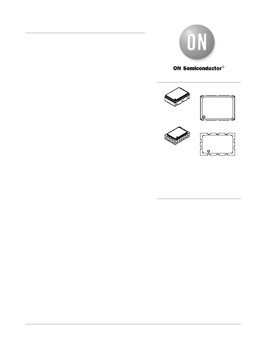
Available in the industry standard 5.0 x 7.0 x 1.8 mm and in a new
smaller 3.2 x 5.0 x 1.2 mm SMD (CLCC) package on 16 mm tape and
reel in quantities of 1,000.
Features
LVDS Differential Output
Uses High Q Fundamental Mode Crystal
Ultra Low Jitter and Phase Noise 0.5 ps (12 kHz 20 MHz)
Factory Configurable Frequencies from 60 MHz to 700 MHz (see
Standard Frequencies in the Ordering Information Table on page 6)
Pullable Range Minimum of ±100 ppm
Frequency Stability of ±50 ppm
Control Voltage with Positive Slope
Voltage Control Linearity of ±10%
Hermetically Sealed Ceramic SMD Packages of size 5.0 x 7.0 x
1.8 mm and 3.2 x 5.0 x 1.2 mm
Operating Range: 3.3 V ±10%
These Devices are PbFree and are RoHS Compliant
Applications
Networking
SONET
10 Gigabit Ethernet
Networking Base Stations
Broadcasting
http://onsemi.com
MARKING DIAGRAMS
NBVSPXXXX = NBVSPXXXX (±50 ppm)
XXX.XXXX
= Output Frequency (MHz)
A
= Assembly Location
WL
= Wafer Lot
YY
= Year
WW
= Work Week
G
= PbFree Package
6 PIN CLCC
LN SUFFIX
CASE 848AB
NBVSPXXXX
XXX.XXXX
AWLYYWWG
6 PIN CLCC
LU SUFFIX
CASE 848AC
NBVSPXXXX
XXX.XXXX
AWLYYWWG
See detailed ordering and shipping information in the package
dimensions section on page 6 of this data sheet.
ORDERING INFORMATION
相關(guān)PDF資料 |
PDF描述 |
|---|---|
| VI-B5N-IU-F2 | CONVERTER MOD DC/DC 18.5V 200W |
| NBVSBA027LNHTAG | IC VCXO LVPECL 148.5MHZ 6CLCC |
| DS1077U-100+T&R | IC ECONOSCILLATOR 100MHZ 8-USOP |
| DS1077U-120+T&R | IC ECONOSCILLATOR 120MHZ 8-USOP |
| MS27656E13A4S | CONN RCPT 4POS WALL MNT W/SCKT |
相關(guān)代理商/技術(shù)參數(shù) |
參數(shù)描述 |
|---|---|
| NBVSPA018LN1TAG | 功能描述:VCXO振蕩器 VCXO LVDS 155.52 MHZ RoHS:否 制造商:Fox 封裝 / 箱體:5 mm x 3.2 mm 頻率:19.2 Mhz 頻率穩(wěn)定性:2.5 PPM 輸出格式: 封裝:Reel 電源電壓:3 V 端接類型:SMD/SMT 尺寸:3.2 mm W x 5 mm L x 1.5 mm H 最小工作溫度:- 20 C 最大工作溫度:+ 75 C |
| NBVSPA018LNHTAG | 功能描述:VCXO振蕩器 2.5/3.3 V 155.52 MHZ LVDS PureEdge RoHS:否 制造商:Fox 封裝 / 箱體:5 mm x 3.2 mm 頻率:19.2 Mhz 頻率穩(wěn)定性:2.5 PPM 輸出格式: 封裝:Reel 電源電壓:3 V 端接類型:SMD/SMT 尺寸:3.2 mm W x 5 mm L x 1.5 mm H 最小工作溫度:- 20 C 最大工作溫度:+ 75 C |
| NBVSPA019LN1TAG | 功能描述:VCXO振蕩器 VCXO LVDS 125 MHZ RoHS:否 制造商:Fox 封裝 / 箱體:5 mm x 3.2 mm 頻率:19.2 Mhz 頻率穩(wěn)定性:2.5 PPM 輸出格式: 封裝:Reel 電源電壓:3 V 端接類型:SMD/SMT 尺寸:3.2 mm W x 5 mm L x 1.5 mm H 最小工作溫度:- 20 C 最大工作溫度:+ 75 C |
| NBVSPA019LNHTAG | 功能描述:VCXO振蕩器 3.3V 125.00 MHZ LVDS PureEdge RoHS:否 制造商:Fox 封裝 / 箱體:5 mm x 3.2 mm 頻率:19.2 Mhz 頻率穩(wěn)定性:2.5 PPM 輸出格式: 封裝:Reel 電源電壓:3 V 端接類型:SMD/SMT 尺寸:3.2 mm W x 5 mm L x 1.5 mm H 最小工作溫度:- 20 C 最大工作溫度:+ 75 C |
| NBVSPA024LN1TAG | 功能描述:VCXO振蕩器 VCXO LVDS 160 MHZ RoHS:否 制造商:Fox 封裝 / 箱體:5 mm x 3.2 mm 頻率:19.2 Mhz 頻率穩(wěn)定性:2.5 PPM 輸出格式: 封裝:Reel 電源電壓:3 V 端接類型:SMD/SMT 尺寸:3.2 mm W x 5 mm L x 1.5 mm H 最小工作溫度:- 20 C 最大工作溫度:+ 75 C |
發(fā)布緊急采購(gòu),3分鐘左右您將得到回復(fù)。