- 您現(xiàn)在的位置:買(mǎi)賣(mài)IC網(wǎng) > PDF目錄4569 > NBSG16VSMAG (ON Semiconductor)IC RCVR/DRVR SIGE DIFF 16-FCLGA PDF資料下載
參數(shù)資料
| 型號(hào): | NBSG16VSMAG |
| 廠(chǎng)商: | ON Semiconductor |
| 文件頁(yè)數(shù): | 14/14頁(yè) |
| 文件大?。?/td> | 0K |
| 描述: | IC RCVR/DRVR SIGE DIFF 16-FCLGA |
| 產(chǎn)品變化通告: | Product Discontinuation 04/April/2008 |
| 標(biāo)準(zhǔn)包裝: | 92 |
| 類(lèi)型: | 收發(fā)器 |
| 應(yīng)用: | 儀表 |
| 安裝類(lèi)型: | 表面貼裝 |
| 封裝/外殼: | 16-VFQFN 裸露焊盤(pán) |
| 供應(yīng)商設(shè)備封裝: | 16-QFN(3x3) |
| 包裝: | 管件 |
第1頁(yè)第2頁(yè)第3頁(yè)第4頁(yè)第5頁(yè)第6頁(yè)第7頁(yè)第8頁(yè)第9頁(yè)第10頁(yè)第11頁(yè)第12頁(yè)第13頁(yè)當(dāng)前第14頁(yè)
NBSG16VS
http://onsemi.com
9
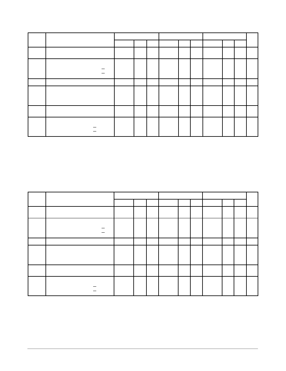
Table 10. AC CHARACTERISTICS for QFN16 VCC = 0 V; VEE = 3.465 V to 3.0 V or VCC = 3.0 V to 3.465 V; VEE = 0 V
Symbol
Characteristic
40°C
25°C
85°C
Unit
Min
Typ
Max
Min
Typ
Max
Min
Typ
Max
fmax
Maximum Frequency
10
(Note 37)
12
10
(Note 37)
12
10
(Note 37)
12
GHz
tPLH,
tPHL
Propagation Delay to
Output Differential
(VCTRL = VCC 2 V) D → Q, Q
(VCTRL = VCC 1 V) D → Q, Q
100
140
135
180
100
140
135
180
100
80
140
135
180
220
ps
tSKEW
Duty Cycle Skew (Note 35)
3
20
3
15
3
10
ps
tJITTER
RMS Random Clock Jitter
fin < 10 GHz
PeaktoPeak Data Dependent Jitter
fin < 10 Gb/s
0.5
TBD
2
0.5
TBD
2
0.5
TBD
2
ps
VINPP
Input Voltage Swing/Sensitivity
(Differential Configuration) (Note 36)
75
2600
75
2600
75
2600
mV
tr
tf
Output Rise/Fall Times (20% 80%)
@ 1 GHz
(VCTRL = VCC 2 V) Q, Q
(VCTRL = VCC 1 V) Q, Q
30
45
40
55
50
30
45
40
55
50
30
45
40
55
50
ps
NOTE: Device will meet the specifications after thermal equilibrium has been established when mounted in a test socket or printed circuit
board with maintained transverse airflow greater than 500 lfpm. Electrical parameters are guaranteed only over the declared
operating temperature range. Functional operation of the device exceeding these conditions is not implied. Device specification limit
values are applied individually under normal operating conditions and not valid simultaneously.
34.Measured using a 500 mV source, 50% duty cycle clock source. All loading with 50 W to VCC2.0 V. Input edge rates 40 ps (20% 80%).
36.VINPP(MAX) cannot exceed VCC VEE (applicable only when VCC VEE t 2600 mV).
37.Conditions include input amplitude of 500 mV and VCTRL = VCC 2 V. Minimum output amplitude guarantee of 100 mV (see Output PP
Spec in Figure 8).
Table 11. AC CHARACTERISTICS for QFN16 VCC = 0 V; 3.0 V tVEE v 2.375 V or 2.375 V v VCC t 3.0 V; VEE = 0 V
Symbol
Characteristic
40°C
25°C
85°C
Unit
Min
Typ
Max
Min
Typ
Max
Min
Typ
Max
fmax
Maximum Frequency
10
(Note 41)
12
10
(Note 41)
12
10
(Note 41)
12
GHz
tPLH,
tPHL
Propagation Delay to
Output Differential
(VCTRL = VCC 2 V) D → Q, Q
(VCTRL = VCC 1 V) D → Q, Q
100
140
135
180
100
140
135
180
80
100
140
135
180
220
ps
tSKEW
Duty Cycle Skew (Note 39)
3
20
3
15
3
10
ps
tJITTER
RMS Random Clock Jitter
fin < 10 GHz
PeaktoPeak Data Dependent Jitter
fin < 10 Gb/s
0.5
TBD
3
0.5
TBD
3
0.5
TBD
3
ps
VINPP
Input Voltage Swing/Sensitivity
(Differential Configuration) (Note 40)
75
2600
75
2600
75
2600
mV
tr
tf
Output Rise/Fall Times (20% 80%)
@ 1 GHz
(VCTRL = VCC 2 V) Q, Q
(VCTRL = VCC 1 V) Q, Q
25
22
50
45
70
60
25
22
50
45
70
60
25
22
50
45
70
60
ps
NOTE: Device will meet the specifications after thermal equilibrium has been established when mounted in a test socket or printed circuit
board with maintained transverse airflow greater than 500 lfpm. Electrical parameters are guaranteed only over the declared
operating temperature range. Functional operation of the device exceeding these conditions is not implied. Device specification limit
values are applied individually under normal operating conditions and not valid simultaneously.
38.Measured using a 500 mV source, 50% duty cycle clock source. All loading with 50 W to VCC2.0 V. Input edge rates 40 ps (20% 80%).
40.VINPP(MAX) cannot exceed VCC VEE (applicable only when VCC VEE t 2600 mV).
41.Conditions include input amplitude of 500 mV and VCTRL = VCC 2 V. Minimum output amplitude guarantee of 100 mV (see Output PP
Spec in Figure 9).
相關(guān)PDF資料 |
PDF描述 |
|---|---|
| CS8190EDWF20 | IC TACH/SPEEDO DRVR PREC 20SOICW |
| MCZ79076EG | IC IGNITION CTRL ELECTR 16-SOIC |
| MC33780EGR2 | IC DBUS MASTER DUAL DIFF 16-SOIC |
| MC44BS373CAFC | IC MODULATOR AUD/VID U/V 20-QFN |
| LFX200EB-03F256C | IC FPGA 200K GATES 256-BGA |
相關(guān)代理商/技術(shù)參數(shù) |
參數(shù)描述 |
|---|---|
| NBSG16VSMN | 功能描述:緩沖器和線(xiàn)路驅(qū)動(dòng)器 2.5V/3.3V SiGe Diff RoHS:否 制造商:Micrel 輸入線(xiàn)路數(shù)量:1 輸出線(xiàn)路數(shù)量:2 極性:Non-Inverting 電源電壓-最大:+/- 5.5 V 電源電壓-最小:+/- 2.37 V 最大工作溫度:+ 85 C 安裝風(fēng)格:SMD/SMT 封裝 / 箱體:MSOP-8 封裝:Reel |
| NBSG16VSMNG | 功能描述:緩沖器和線(xiàn)路驅(qū)動(dòng)器 2.5V/3.3V SiGe Diff w/Variable Output RoHS:否 制造商:Micrel 輸入線(xiàn)路數(shù)量:1 輸出線(xiàn)路數(shù)量:2 極性:Non-Inverting 電源電壓-最大:+/- 5.5 V 電源電壓-最小:+/- 2.37 V 最大工作溫度:+ 85 C 安裝風(fēng)格:SMD/SMT 封裝 / 箱體:MSOP-8 封裝:Reel |
| NBSG16VSMNHTBG | 功能描述:緩沖器和線(xiàn)路驅(qū)動(dòng)器 BBG 2.5V/3.3V SIGE DIFF RoHS:否 制造商:Micrel 輸入線(xiàn)路數(shù)量:1 輸出線(xiàn)路數(shù)量:2 極性:Non-Inverting 電源電壓-最大:+/- 5.5 V 電源電壓-最小:+/- 2.37 V 最大工作溫度:+ 85 C 安裝風(fēng)格:SMD/SMT 封裝 / 箱體:MSOP-8 封裝:Reel |
| NBSG16VSMNR2 | 功能描述:緩沖器和線(xiàn)路驅(qū)動(dòng)器 2.5V/3.3V SiGe Diff RoHS:否 制造商:Micrel 輸入線(xiàn)路數(shù)量:1 輸出線(xiàn)路數(shù)量:2 極性:Non-Inverting 電源電壓-最大:+/- 5.5 V 電源電壓-最小:+/- 2.37 V 最大工作溫度:+ 85 C 安裝風(fēng)格:SMD/SMT 封裝 / 箱體:MSOP-8 封裝:Reel |
| NBSG16VSMNR2G | 功能描述:緩沖器和線(xiàn)路驅(qū)動(dòng)器 2.5V/3.3V SiGe Diff w/Variable Output RoHS:否 制造商:Micrel 輸入線(xiàn)路數(shù)量:1 輸出線(xiàn)路數(shù)量:2 極性:Non-Inverting 電源電壓-最大:+/- 5.5 V 電源電壓-最小:+/- 2.37 V 最大工作溫度:+ 85 C 安裝風(fēng)格:SMD/SMT 封裝 / 箱體:MSOP-8 封裝:Reel |
發(fā)布緊急采購(gòu),3分鐘左右您將得到回復(fù)。