- 您現(xiàn)在的位置:買賣IC網(wǎng) > PDF目錄2038 > NB4L52MNR2G (ON Semiconductor)IC FLIP FLOP DATA/CLK DFF 16-QFN PDF資料下載
參數(shù)資料
| 型號(hào): | NB4L52MNR2G |
| 廠商: | ON Semiconductor |
| 文件頁數(shù): | 2/8頁 |
| 文件大?。?/td> | 0K |
| 描述: | IC FLIP FLOP DATA/CLK DFF 16-QFN |
| 標(biāo)準(zhǔn)包裝: | 3,000 |
| 功能: | 復(fù)位 |
| 類型: | D 型 |
| 輸出類型: | 差分 |
| 元件數(shù): | 1 |
| 每個(gè)元件的位元數(shù): | 1 |
| 延遲時(shí)間 - 傳輸: | 400ps |
| 觸發(fā)器類型: | 負(fù)邊沿 |
| 電源電壓: | 2.3 V ~ 5.5 V |
| 工作溫度: | -40°C ~ 85°C |
| 安裝類型: | 表面貼裝 |
| 封裝/外殼: | 16-VFQFN 裸露焊盤 |
| 包裝: | 帶卷 (TR) |
NB4L52
http://onsemi.com
2
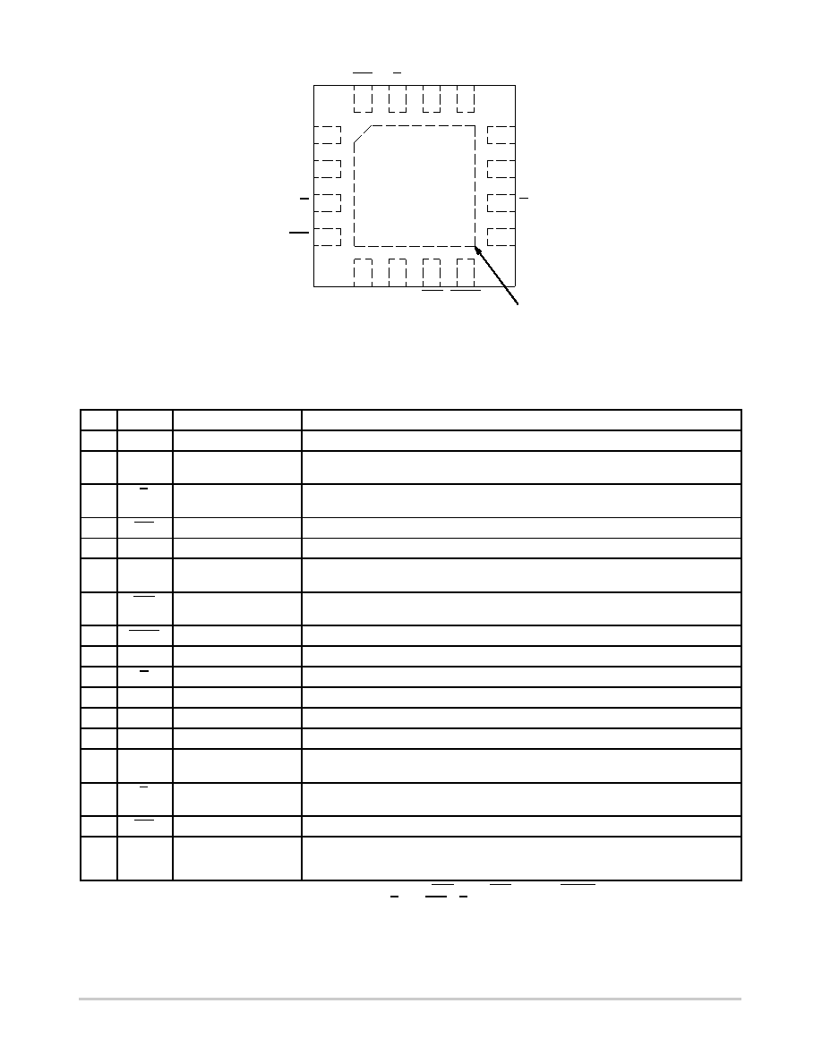
R
Figure 2. Pinout (Top View)
D
VTD
VCC
Q
CLK
Q
VTCLK
VEE
1
2
3
4
5
678
9
10
11
12
13
14
15
16
VTR
R
CLK
NB4L52
VTR
Exposed Pad (EP)
VTCLK
Table 2. PIN DESCRIPTION
Pin
Name
I/O
Description
1
VTD
Internal 50 W Termination Pin. (See Table 4)
2
D
ECL, CML, LVCMOS,
LVDS, LVTTL Input
Noninverted Differential Input. (Note 1)
3
D
ECL, CML, LVCMOS,
LVDS, LVTTL Input
Inverted Differential Input. (Note 1)
4
VTD
Internal 50 W Termination Pin. (See Table 4)
5
VTCLK
Internal 50 W Termination Pin. (See Table 4)
6
CLK
ECL, CML, LVCMOS,
LVDS, LVTTL Input
Noninverted Differential Input. (Note 1)
7
CLK
ECL, CML, LVCMOS,
LVDS, LVTTL Input
Inverted Differential Input. (Note 1)
8
VTCLK
Internal 50 W Termination Pin. (See Table 4)
9
VEE
Negative Supply Voltage
10
Q
ECL Output
Inverted Differential Output. Typically terminated with 50 W resistor to VCC 2.0 V.
11
Q
ECL Output
Noninverted Differential Output. Typically terminated with 50 W resistor to VCC 2.0 V.
12
VCC
Positive Supply Voltage
13
VTR
Internal 50 W Termination Pin. (See Table 4)
14
R
LVECL, LVCMOS,
LVTTL Input
Noninverted Differential Reset Input. (Note 1)
15
R
LVECL, LVCMOS,
LVTTL Input
Inverted Differential Reset Input. (Note 1)
16
VTR
Internal 50 W Termination Pin. (See Table 4)
EP
The Exposed Pad (EP) on the QFN16 package bottom is thermally connected to the die
for improved heat transfer out of package. The pad is not electrically connected to the die,
but is recommended to be electrically and thermally connected to VEE on the PC board.
1. In the differential configuration when the input termination pin (VTD, VTD, VTR, VTR, VTCLK, VTCLK) are connected to a common
termination voltage or left open, and if no signal is applied on D/D,CLK/CLK,R/R input then the device will be susceptible to selfoscillation.
相關(guān)PDF資料 |
PDF描述 |
|---|---|
| NB7V52MMNHTBG | IC FLIP FLOP DATA/CLOCK D 16-QFN |
| NBSG53ABAHTBG | IC CLOCK/DATA DIFF DIV/2 16FCBGA |
| NC7SP74L8X | IC FLIP FLOP ULP D 8-MICROPAK |
| NC7SZ175P6X_F40 | IC FLIP FLOP SGL UHS D SC70-6 |
| NC7SZ373P6 | IC LATCH UHS D 3-STATE SC70-6 |
相關(guān)代理商/技術(shù)參數(shù) |
參數(shù)描述 |
|---|---|
| NB4L6254 | 制造商:ONSEMI 制造商全稱:ON Semiconductor 功能描述:2.5V / 3.3V Differential LVPECL 2x2 Clock Switch and Low Skew Fanout Buffer |
| NB4L6254D | 制造商:ONSEMI 制造商全稱:ON Semiconductor 功能描述:2.5V / 3.3V Differential LVPECL 2x2 Clock Switch and Low Skew Fanout Buffer |
| NB4L6254FAG | 功能描述:模擬和數(shù)字交叉點(diǎn) IC LVPECL 2X2 SW FANOUT RoHS:否 制造商:Micrel 配置:2 x 2 封裝 / 箱體:MLF-16 數(shù)據(jù)速率:10.7 Gbps 輸入電平:CML, LVDS, LVPECL 輸出電平:CML 電源電壓-最大:3.6 V 電源電壓-最小:2.375 V 最大工作溫度:+ 85 C 最小工作溫度:- 40 C 產(chǎn)品:Digital Crosspoint 封裝:Tube |
| NB4L6254FAR2G | 功能描述:模擬和數(shù)字交叉點(diǎn) IC AIT LVPECL 2X2 SW FN RoHS:否 制造商:Micrel 配置:2 x 2 封裝 / 箱體:MLF-16 數(shù)據(jù)速率:10.7 Gbps 輸入電平:CML, LVDS, LVPECL 輸出電平:CML 電源電壓-最大:3.6 V 電源電壓-最小:2.375 V 最大工作溫度:+ 85 C 最小工作溫度:- 40 C 產(chǎn)品:Digital Crosspoint 封裝:Tube |
| NB4L6254MNG | 功能描述:時(shí)鐘驅(qū)動(dòng)器及分配 LVPECL 2X2 SWITCH FANOUT RoHS:否 制造商:Micrel 乘法/除法因子:1:4 輸出類型:Differential 最大輸出頻率:4.2 GHz 電源電壓-最大: 電源電壓-最小:5 V 最大工作溫度:+ 85 C 封裝 / 箱體:SOIC-8 封裝:Reel |
發(fā)布緊急采購(gòu),3分鐘左右您將得到回復(fù)。