- 您現(xiàn)在的位置:買賣IC網(wǎng) > PDF目錄384764 > MX7847TQ (MAXIM INTEGRATED PRODUCTS INC) Complete, Dual, 12-Bit Multiplying DACs PDF資料下載
參數(shù)資料
| 型號: | MX7847TQ |
| 廠商: | MAXIM INTEGRATED PRODUCTS INC |
| 元件分類: | DAC |
| 英文描述: | Complete, Dual, 12-Bit Multiplying DACs |
| 中文描述: | DUAL, PARALLEL, WORD INPUT LOADING, 4 us SETTLING TIME, 12-BIT DAC, CDIP24 |
| 封裝: | CERDIP-24 |
| 文件頁數(shù): | 3/12頁 |
| 文件大?。?/td> | 168K |
| 代理商: | MX7847TQ |
M
Complete, Dual, 12-Bit
Multiplying DACs
_______________________________________________________________________________________
3
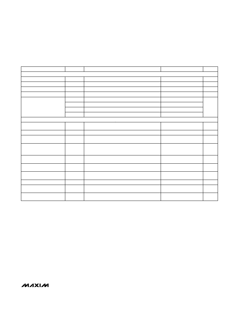
PARAMETER
POWER REQUIREMENTS
SYMBOL
MIN
TYP
MAX
UNITS
CONDITIONS
±0.01
±0.01
±0.01
±0.01
Power-Supply Rejection
% per %
Voltage-Output Settling
Time
Slew Rate
Digital-to Analog Glitch
Impulse
Channel-to-Channel Isolation
(V
REFA
to V
OUTB
,
V
REFB
to V
OUTA
)
Multiplying Feedthrough
Error
Unity-Gain Small-Signal
Bandwidth
t
S
Settling time to within ±1/2LSB of final DAC value;
DAC latch alternately loaded will all 0s and all 1s
4
μs
7
V/μs
Q
DAC latch alternately loaded with 01…11 and
10…00
60
nV-s
V
REF
= 20p-p, 10kHz sine wave, Alternate DAC
Latch Loaded with all 0s
-95
dB
-90
dB
THD
1
MHz
Full-Power Bandwidth
125
kHz
Total Harmonic Distortion
V
REF
= 6V
RMS
, 1kHz, DAC latch loaded with all 1s
Code transition from all 0s to all 1s; see Typical
Operating Characteristics graphs
-88
dB
Digital Crosstalk
10
nV-s
Output Noise Voltage at
+25°C (0.1Hz to 10Hz)
Amplifier noise and J ohnson noise of R
FB
2
μV
RMS
V
DD
Range
V
SS
Range
V
DD
V
SS
11.4
-11.4
16.5
-16.5
V
V
Positive Supply Current
Negative Supply Current
I
DD
I
SS
5
4
10
6
mA
mA
Output unloaded
Output unloaded
V
DD
= 15V ±5%, V
REF
= -10V
V
REF
= 20V
p-p
S
ine wave, DAC latch loaded with
all 1s
V
REF
= 100mV
p-p
sine wave, DAC latch loaded
with all 1s
V
REF_
= 20V
p-p
, 10kHz sine wave, latches loaded
with all 0s
V
SS
= -12V ±5%, V
REF
= 8.9V
V
DD
= 12V ±5%, V
REF
= -8.9V
V
SS
= -15V ±5%, V
REF
= 10V
Gain/
V
DD
Gain/
V
SS
Gain/
V
DD
Gain/
V
SS
ELECTRICAL CHARACTERISTICS (continued)
(V
DD
= 11.4V to 16.5V, V
SS
= -11.4V to -16.5V, AGNDA = AGNDB = DGND = 0V, V
REFA
= V
REFB
= +10V, R
L
= 2k
, C
L
= 100pF,
V
OUT
connected to R
FB
(MX7837), T
A
= T
MIN
to T
MAX
, unless otherwise noted.) (Note 1)
Note 2:
The analog outputs can swing to within 2.5V of the supply rails. Hence, for good linearity towards full-scale, |V
REFA
|and |V
REFB
|must
be at least 2.5V lower than V
DD
and |V
SS
| Tests done with supply voltages below ±12.5V are done with V
REFA
= V
REFB
= ±8.9V.
Note 3:
Static performance tested at V
DD
= +15V, V
SS
= -15V. Performance over supplies guaranteed by PSRR test.
Note 4:
Guaranteed by design.
AC CHARACTERISTICS
相關(guān)PDF資料 |
PDF描述 |
|---|---|
| MX7845 | Complete, 12-Bit Multiplying DAC |
| MX7845AEWG | Complete, 12-Bit Multiplying DAC |
| MX7845AQ | Complete, 12-Bit Multiplying DAC |
| MX7845BEWG | Complete, 12-Bit Multiplying DAC |
| MX7845BQ | Complete, 12-Bit Multiplying DAC |
相關(guān)代理商/技術(shù)參數(shù) |
參數(shù)描述 |
|---|---|
| MX7847TQ/883B | 制造商:Maxim Integrated Products 功能描述:- Bulk |
| MX7-93PL-C4 | 功能描述:汽車連接器 R/A Pin HEADER 93P RoHS:否 制造商:Amphenol SINE Systems 產(chǎn)品:Contacts 系列:ATP 位置數(shù)量: 型式:Female 安裝風格: 端接類型: 觸點電鍍:Nickel |
| MX7-A-26SC | 制造商:Japan Aviation Electronics (JAE) 功能描述: |
| MX7-A-26S-RT | 制造商:Japan Aviation Electronics (JAE) 功能描述: |
| MX7-A-28SC | 功能描述:汽車連接器 Sckt HOUSING 28P RoHS:否 制造商:Amphenol SINE Systems 產(chǎn)品:Contacts 系列:ATP 位置數(shù)量: 型式:Female 安裝風格: 端接類型: 觸點電鍍:Nickel |
發(fā)布緊急采購,3分鐘左右您將得到回復(fù)。