- 您現(xiàn)在的位置:買賣IC網(wǎng) > PDF目錄383643 > MT8964 (Mitel Networks Corporation) Integrated PCM Filter Codec(集成PCM濾波器/編解碼器(用于數(shù)字遠程通信)) PDF資料下載
參數(shù)資料
| 型號: | MT8964 |
| 廠商: | Mitel Networks Corporation |
| 元件分類: | Codec |
| 英文描述: | Integrated PCM Filter Codec(集成PCM濾波器/編解碼器(用于數(shù)字遠程通信)) |
| 中文描述: | 集成濾波器的PCM編解碼器(集成的PCM濾波器/編解碼器(用于數(shù)字遠程通信)) |
| 文件頁數(shù): | 6/24頁 |
| 文件大?。?/td> | 120K |
| 代理商: | MT8964 |
MT8960/61/62/63/64/65/66/67
ISO
2
-CMOS
6-24
Internally the codec will then perform a decode cycle
on the newly input PCM word. The sampled and
held analog signal thus decoded will be updated 25
μ
s from the start of the cycle. After this the analog
input from the filter is sampled for 18
μ
s, after which
digital conversion takes place during the remaining
82
μ
s of the sampling cycle.
Since a single clock frequency of 2.048 MHz is
required, all digital data is input and output at this
rate. DSTo, therefore, assumes a high impedance
state for all but 3.9
μ
s of the 125
μ
s frame. Similarly,
DSTi input data is valid for only 3.9
μ
s.
Digital Control Functions
CSTi is a digital input (levels GNDD to V
DD
) which is
used to control the function of the filter/codec. It
operates in three different modes depending on the
logic levels applied to the Control Address input
(CA) and chip enable input (F1i) (see Table 1).
Mode 1
CA=-5V (V
EE
); CSTi=0V (GNDD)
The filter/codec is in normal operation with nominal
transmit and receive gain of 0dB. The SD outputs
are in their active states and the test modes cannot
be entered.
CA = -5V (V
EE
); CSTi = +5V (V
DD
)
A state of powerdown is forced upon the chip
whereby DSTo becomes high impedance, V
R
is
connected to GNDA and all analog sections have
power removed.
Mode 2
CA= -5V (V
EE
); CSTi receives an eight-bit control
word
CSTi accepts a serial data stream synchronously
with DSTi (i.e., it accepts an eight-bit serial word in a
3.9
μ
s timeslot, updated every 125
μ
s, and is
specified
identically
to
considerations). This eight-bit control word is
entered into Control Register A and enables
programming of the following functions: transmit and
receive gain, powerdown, loopback. Register B is
reset to zero and the SD outputs assume their
inactive state. Test modes cannot be entered.
DSTi
for
timing
Mode 3
CA=0V (GNDD); CSTi receives an eight-bit control
word
As in Mode 2, the control word enters Register A and
the aforementioned functions are controlled. In this
mode, however, Register B is not reset, thus not
affecting the states of the SD outputs.
CA=+5V (V
DD
); CSTi receives an 8-bit control word
In this case the control word is transferred into
Register B. Register A is unaffected. The input and
output of PCM data is inhibited.
The contents of Register B controls the six
uncommitted outputs SD0-SD5 (four outputs, SD0-
SD3, on MT8960/61/64/65 versions of chip) and also
provide entry into one of the three test modes of the
chip.
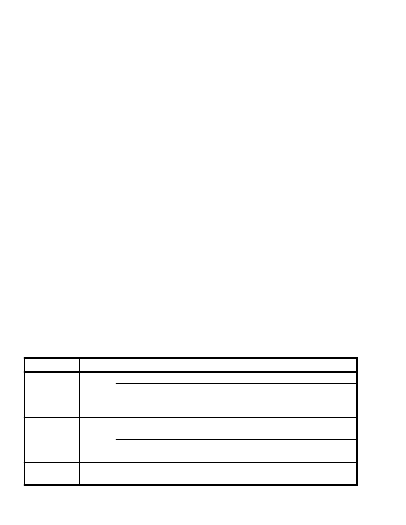
Table 1. Digital Control Modes
MODE
CA
CSTi
FUNCTION
1
(Note 1)
V
EE
GNDD
Normal chip operation.
V
DD
Serial
Powerdown.
2
V
EE
Eight-bit control word into Register A. Register B is reset.
Data
3
(Note 2)
GNDD
Serial
Eight-bit control word into register A. Register B is unaffected.
Data
V
DD
Serial
Eight-bit control word into register A. Register B is unaffected.
Data
Note 1:
When operating in Mode 1, there should be only one frame pulse (F1i) per 125
μ
s frame
When operating in Mode 3, PCM input and output is inhibited by CA=V
DD
.
Note 2:
相關PDF資料 |
PDF描述 |
|---|---|
| MT8965 | Integrated PCM Filter Codec(集成PCM濾波器/編解碼器(用于數(shù)字遠程通信)) |
| MT8966 | Integrated PCM Filter Codec(集成PCM濾波器/編解碼器(用于數(shù)字遠程通信)) |
| MT8971B | ISO2-CMOS ST-BUS⑩ FAMILY Digital Subscriber Interface Circuit Digital Network Interface Circuit |
| MT8971BE | ISO2-CMOS ST-BUS⑩ FAMILY Digital Subscriber Interface Circuit Digital Network Interface Circuit |
| MT8971BP | ISO2-CMOS ST-BUS⑩ FAMILY Digital Subscriber Interface Circuit Digital Network Interface Circuit |
相關代理商/技術參數(shù) |
參數(shù)描述 |
|---|---|
| MT8964AC | 制造商:MITEL 制造商全稱:Mitel Networks Corporation 功能描述:Integrated PCM Filter Codec |
| MT8964AE | 制造商:Microsemi Corporation 功能描述:U-LAW FILTER CODEC EOL190808 制造商:MITEL 功能描述: |
| MT8964AE1 | 制造商:Microsemi Corporation 功能描述: 制造商:Microsemi Corporation 功能描述:PCM FLTR CODEC 18PDIP - Rail/Tube 制造商:MICROSEMI CONSUMER MEDICAL PRODUCT GROUP 功能描述:IC CODEC U-LAW CCITT PCM 18PDIP 制造商:Microsemi Corporation 功能描述:MT8964 Series 5 V 8-bit 1ADC /1 DAC Integrated PCM Filter Codec - PDIP-18 |
| MT8965 | 制造商:MITEL 制造商全稱:Mitel Networks Corporation 功能描述:Integrated PCM Filter Codec |
| MT8965AC | 制造商:MITEL 制造商全稱:Mitel Networks Corporation 功能描述:ISO2-CMOS Integrated PCM Filter Codec |
發(fā)布緊急采購,3分鐘左右您將得到回復。