- 您現(xiàn)在的位置:買(mǎi)賣(mài)IC網(wǎng) > PDF目錄359736 > MT88E45 (Mitel Networks Corporation) 4-Wire Calling Number Identification Circuit 2(4-Wire CNIC2) PDF資料下載
參數(shù)資料
| 型號(hào): | MT88E45 |
| 廠商: | Mitel Networks Corporation |
| 英文描述: | 4-Wire Calling Number Identification Circuit 2(4-Wire CNIC2) |
| 中文描述: | 4線(xiàn)來(lái)電號(hào)碼識(shí)別電路2(4線(xiàn)CNIC2) |
| 文件頁(yè)數(shù): | 3/30頁(yè) |
| 文件大小: | 523K |
| 代理商: | MT88E45 |
第1頁(yè)第2頁(yè)當(dāng)前第3頁(yè)第4頁(yè)第5頁(yè)第6頁(yè)第7頁(yè)第8頁(yè)第9頁(yè)第10頁(yè)第11頁(yè)第12頁(yè)第13頁(yè)第14頁(yè)第15頁(yè)第16頁(yè)第17頁(yè)第18頁(yè)第19頁(yè)第20頁(yè)第21頁(yè)第22頁(yè)第23頁(yè)第24頁(yè)第25頁(yè)第26頁(yè)第27頁(yè)第28頁(yè)第29頁(yè)第30頁(yè)
MT88E45
Data Sheet
3
Zarlink Semiconductor Inc.
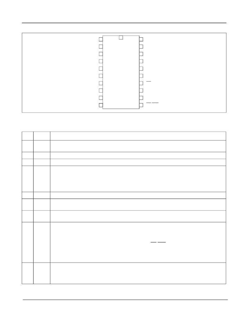
Figure 2 - Pin Connections
Pin Description
Pin #
Name
Description
1
V
REF
Voltage Reference (Output).
Nominally Vdd/2. It is used to bias the Tip/Ring and Hybrid input op-
amps.
2
IN1+
Tip/Ring Op-amp Non-inverting (Input).
3
IN1-
Tip/Ring Op-amp Inverting (Input).
4
GS1
Tip/Ring Gain Select (Output).
This is the output of the Tip/Ring connection op-amp. The op-
amp should be used to connect the MT88E45B to Tip and Ring. The Tip/Ring signal can be
amplified or attenuated at GS1 via selection of the feedback resistor between GS1 and IN1-. FSK
demodulation (which is always on Tip/Ring) or CAS detection (for MEI or BT on-hook CLIP) of the
GS1 signal is enabled via the CB1 and CB2 pins. See Tables 1 and 2.
5
Vss
Power supply ground.
6
OSC1
Oscillator (Input).
Crystal connection. This pin can also be driven directly from an external clock
source.
7
OSC2
Oscillator (Output).
Crystal connection. When OSC1 is driven by an external clock, this pin
should be left open.
8
CB0
Control Bit 0 (CMOS Input)
. This pin is used primarily to select the 3-wire FSK data interface
mode. When it is low, interface mode 0 is selected where the FSK bit stream is output directly.
When it is high, interface mode 1 is selected where the FSK byte is stored in a 1 byte buffer which
can be read serially by the application’s microcontroller.
The FSK interface is consisted of the DATA, DCLK and DR/STD pins. See the 3 pin descriptions
to understand how CB0 affects the FSK interface.
When CB0 is high and CB1, CB2 are both low the MT88E45B is put into a power down state
consuming minimal power supply current. See Tables 1 and 2.
9
DCLK
3-wire FSK Interface Data Clock (Schmitt Input/CMOS Output).
In mode 0 (when the CB0 pin
is logic low) this is a CMOS output which denotes the nominal mid-point of a FSK data bit.
In mode 1 (when the CB0 pin is logic high) this is a Schmitt trigger input used to shift the FSK data
byte out to the DATA pin.
1
2
3
4
5
6
9
10
20
19
18
17
16
15
14
13
V
REF
IN1+
IN1-
GS1
Vss
OSC1
DCLK
DATA
IN2+
IN2-
GS2
CB2
CB1
Vdd
CD
ST/GT
MT88E45B
7
OSC2
8
CB0
12
11
EST
DR/STD
相關(guān)PDF資料 |
PDF描述 |
|---|---|
| MT88E45AS | 4-Wire Calling Number Identification Circuit 2(4-Wire CNIC2) |
| MAN6710 | 0.560-INCH SEVEN SEGMENT DISPLAYS |
| MAN8410 | 0.800-INCH SEVEN SEGMENT DISPLAYS |
| MAN6410 | 0.560-INCH SEVEN SEGMENT DISPLAYS |
| MSK5151 | VERY HIGH CURRENT, LOW DROPOUT VOLTAGE REGULATORS |
相關(guān)代理商/技術(shù)參數(shù) |
參數(shù)描述 |
|---|---|
| MT88E45AS | 制造商:MITEL 制造商全稱(chēng):Mitel Networks Corporation 功能描述:4-Wire Calling Number Identification Circuit 2(4-Wire CNIC2) |
| MT88E45B | 制造商:ZARLINK 制造商全稱(chēng):Zarlink Semiconductor Inc 功能描述:4-Wire Calling Number Identification Circuit 2 (4-Wire CNIC2) |
| MT88E45BN | 制造商:ZARLINK 制造商全稱(chēng):Zarlink Semiconductor Inc 功能描述:4-Wire Calling Number Identification Circuit 2 |
| MT88E45BN1 | 制造商:Microsemi Corporation 功能描述:CALLER ID CMOS 3.58MHZ 3.3V 20SSOP - Rail/Tube 制造商:MICROSEMI CONSUMER MEDICAL PRODUCT GROUP 功能描述:IC CNIC CIDCW CID 20SSOP 制造商:Microsemi Corporation 功能描述:IC CNIC CIDCW CID 20SSOP |
| MT88E45BNR | 制造商:Microsemi Corporation 功能描述:CALLER ID CMOS 3.58MHZ 3.3V 20SSOP - Tape and Reel |
發(fā)布緊急采購(gòu),3分鐘左右您將得到回復(fù)。