- 您現(xiàn)在的位置:買賣IC網(wǎng) > PDF目錄369933 > MT5C6401 (Austin Semiconductor, Inc) 64K x 1 SRAM SRAM MEMORY ARRAY PDF資料下載
參數(shù)資料
| 型號: | MT5C6401 |
| 廠商: | Austin Semiconductor, Inc |
| 英文描述: | 64K x 1 SRAM SRAM MEMORY ARRAY |
| 中文描述: | 64K的× 1 SRAM的存儲器陣列 |
| 文件頁數(shù): | 1/10頁 |
| 文件大小: | 145K |
| 代理商: | MT5C6401 |

SRAM
MT5C6401
Austin Semiconductor, Inc.
MT5C6401
Rev. 1.0 8/01
Austin Semiconductor, Inc. reserves the right to change products or specifications without notice.
1
FEATURES
Speeds: 12, 15, 20, 25, 35, 45, 55, and 70ns
Battery Backup: 2V data retention
High-performance, low-power CMOS double-metal
process
Single +5V (+10%) Power Supply
Easy memory expansion with CE\
All inputs and outputs are TTL compatible
OPTIONS
Timing
12ns access
15ns access
20ns access
25ns access
35ns access
45ns access
55ns access
70ns access
MARKING
-12
-15
-20
-25
-35
-45*
-55*
-70*
Package(s)
Ceramic DIP (300 mil)
C
No. 105
Operating Temperature Ranges
Industrial (-40
o
C to +85
o
C)
Military (-55
o
C to +125
o
C)
IT
XT
2V data retention/low power
L
*Electrical characteristics identical to those provided for the 35ns
access devices.
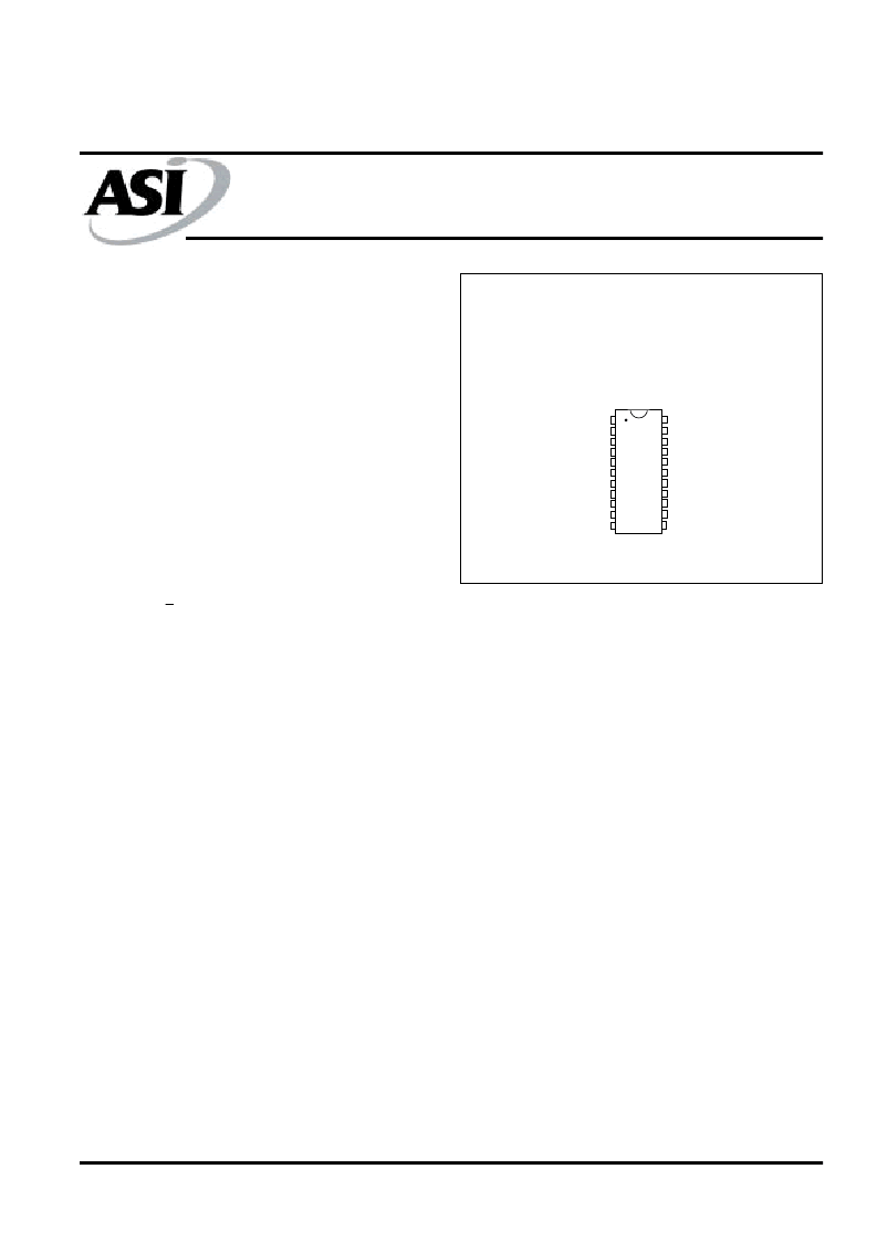
PIN ASSIGNMENT
(Top View)
AVAILABLE AS MILITARY
SPECIFICATIONS
SMD 5962-86015
MIL-STD-883
GENERAL DESCRIPTION
The Austin Semiconductor SRAM family employs
high-speed, low-power CMOS designs using a four-transistor
memory cell. Austin Semiconductor SRAMs are fabricated
using double-layer metal, double-layer polysilicon
technology.
For flexibility in high-speed memory applications, Austin
Semiconductor offers chip enable (CE\) on all organizations.
This enhancement can place the outputs in High-Z for
additional flexibility in system design. The X1 configuration
features separate data input and output.
Writing to these devices is accomplished when write
enable (WE\) and CE\ inputs are both LOW. Reading is
accomplished when WE\ remains HIGH and CE\ goes LOW.
The device offers a reduced power standby mode when
disabled. This allows system designs to achieve low standby
power requirements.
All devices operate from a single +5V power supply and
all inputs and outputs are fully TTL compatible.
64K x 1 SRAM
SRAM MEMORY ARRAY
For more products and information
please visit our web site at
www.austinsemiconductor.com
22-Pin DIP (C)
(300 MIL)
1
2
3
4
5
6
7
8
9
10
11
22
21
20
19
18
17
16
15
14
13
12
A0
A1
A2
A3
A4
A5
A6
A7
Q
WE\
Vss
Vcc
A15
A14
A13
A12
A11
A10
A9
A8
D
CE\
相關(guān)PDF資料 |
PDF描述 |
|---|---|
| MT6C03AE | TOSHIBA TRANSISTOR SILICON NPN EPITAXIAL PLANAR TYPE |
| MT6C04AE | VHF~UHF BAND LOW NOISE AMPLIFIER APPLICATIONS |
| MT6L03AT | TOSHIBA TRANSISTOR SILICON NPN EPITAXIAL PLANAR TYPE |
| MT6L03AE | TOSHIBA TRANSISTOR SILICON NPN EPITAXIAL PLANAR TYPE |
| MT6L04AE | TOSHIBA TRANSISTOR SILICON NPN EPITAXIAL PLANAR TYPE |
相關(guān)代理商/技術(shù)參數(shù) |
參數(shù)描述 |
|---|---|
| MT5C6401DJ25 | 制造商:MICRON 功能描述:* |
| MT5C6404-15 | 制造商:MT 功能描述:Static RAM, 16Kx4, 22 Pin, Plastic, DIP |
| MT5C6404-25 | 制造商:MICRO 功能描述: |
| MT5C6404DJ-20 | 制造商:Micron Technology Inc 功能描述: |
| MT5C6405DJ-20 | 制造商:MICRO CHIP 功能描述: |
發(fā)布緊急采購,3分鐘左右您將得到回復(fù)。