- 您現(xiàn)在的位置:買賣IC網(wǎng) > PDF目錄374529 > MSK5332-10ETS (M.S. Kennedy Corporation) NEGATIVE, 3 AMP, LOW DROPOUT VOLTAGE REGULATOR PDF資料下載
%
%
V
%
%
%
%
mA
mA
A
dB
°C/W
PART
NUMBER
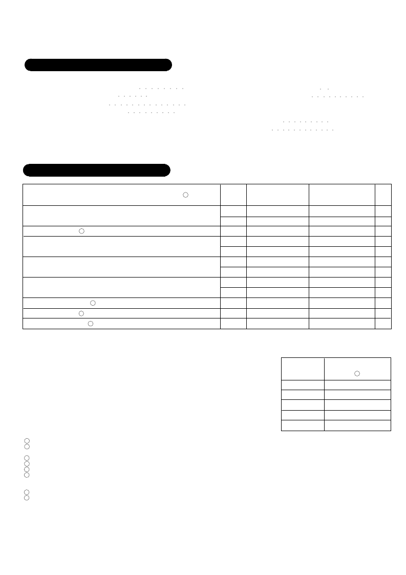
Dropout Voltage
Short Circuit Current
Ripple Rejection
Thermal Resistance
Max.
1.0
2.0
1.2
1.0
2.0
0.5
0.75
10
10
-3.3
-
7.0
Storage Temperature Range
Lead Temperature Range
(10 Seconds)
Case Operating Temperature
MSK 5332H/E
MSK 5332
-30V
Internally Limited
-3A
+175°C
-65°C to +150°C
300°C
-55°C to +125°C
-40°C to +85°C
ABSOLUTE MAXIMUM RATINGS
T
ST
T
LD
T
C
Input Voltage (WRT V
OUT
)
Power Dissipation
Output Current
Junction Temperature
○
○
○
○
○
○
○
○
○
○
○
○
○
○
○
○
○
○
-V
IN
P
D
I
OUT
T
J
○
○
○
○
○
○
○
○
○
○
○
○
○
○
○
○
○
○
○
○
○
○
○
○
○
○
○
○
○
○
○
○
○
○
○
○
○
○
○
○
○
○
○
○
○
○
○
○
○
○
Output is decoupled to ground using 33μF minimum, low ESR capacitors unless otherwise specified.
Guaranteed by design but not tested. Typical parameters are representative of actual device
performance but are for reference only.
All output parameters are tested using a low duty cycle pulse to maintain T
J
= T
C
.
Industrial grade and "E" suffix devices shall be tested to subgroup 1 unless otherwise specified.
Military grade devices ("H" suffix) shall be 100% tested to subgroups 1,2 and 3.
Subgroup 1 T
A
=T
C
=+25°C
2 T
A
=T
C
=+125°C
3 T
A
=T
C
=-55°C
Please consult the factory if alternate output voltages are required.
Input voltage (V
IN
= V
OUT
+ a specified voltage) is implied to be more negative than V
OUT
.
Min.
-
-
-
-
-
-
-
-
-
-
60
-
Group A
Subgroup
1
2,3
1
1
2,3
1
2,3
1
2,3
-
-
-
Min.
-
-
-
-
-
-
-
-
-
-
60
-
Typ.
0.1
0.1
0.8
0.2
0.3
0.1
0.2
4.5
4.5
-3.6
75
5.6
Typ.
0.1
-
0.8
0.2
-
0.1
-
4.5
-
-3.6
75
5.6
Max.
2.0
-
1.3
2.0
-
0.6
-
12
-
-3.0
-
7.5
Parameter
ELECTRICAL SPECIFICATIONS
Test Conditions
Units
MSK 5332
MSK 5332H/E
3
2
2
0A
≤
I
OUT
≤
3A;
V
OUT
=1%
10mA
≤
I
OUT
≤
3A
V
IN
=V
OUT
+3V
I
OUT
=10mA
(V
OUT
+3V)
≤
V
IN
≤
(V
OUT
+15V)
V
IN
=V
OUT
+5V
I
OUT
=3A; C
OUT
=25μF; f=120Hz
JUNCTION TO CASE @ 125°C
-5.0V
-5.2V
-10.0V
-12.0V
-15.0V
MSK5332-5.0
MSK5332-5.2
MSK5332-10
MSK5332-12
MSK5332-15
OUTPUT VOLTAGE
7
2
Rev. B 8/05
1
2
3
4
5
6
7
8
2
NOTES:
○
○
Output Voltage Tolerance
Load Regulation
Line Regulation
I
OUT
=10mA; V
IN
=V
OUT
+3V
Quiescent Current
V
IN
=V
OUT
+3V; I
OUT
=10mA
2
相關(guān)PDF資料 |
PDF描述 |
|---|---|
| MSK5332-10ETU | NEGATIVE, 3 AMP, LOW DROPOUT VOLTAGE REGULATOR |
| MSK5332-10EU | NEGATIVE, 3 AMP, LOW DROPOUT VOLTAGE REGULATOR |
| MSK5332-10G | NEGATIVE, 3 AMP, LOW DROPOUT VOLTAGE REGULATOR |
| MSK5332-10HD | NEGATIVE, 3 AMP, LOW DROPOUT VOLTAGE REGULATOR |
| MSK5332-10HG | NEGATIVE, 3 AMP, LOW DROPOUT VOLTAGE REGULATOR |
相關(guān)代理商/技術(shù)參數(shù) |
參數(shù)描述 |
|---|---|
| MSK600 | 制造商:MSK 制造商全稱:M.S. Kennedy Corporation 功能描述:WIDE BANDWIDTH HIGH VOLTAGE AMPLIFIER |
| MSK601 | 制造商:MSK 制造商全稱:M.S. Kennedy Corporation 功能描述:WIDE BANDWIDTH HIGH VOLTAGE AMPLIFIER |
| MSK601B | 制造商:MSK 制造商全稱:M.S. Kennedy Corporation 功能描述:WIDE BANDWIDTH HIGH VOLTAGE AMPLIFIER |
| MSK604 | 制造商:MSK 制造商全稱:M.S. Kennedy Corporation 功能描述:NEGATIVE OUTPUT WIDE BANDWIDTH HIGH VOLTAGE AMPLIFIER |
| MSK604B | 制造商:MSK 制造商全稱:M.S. Kennedy Corporation 功能描述:NEGATIVE OUTPUT WIDE BANDWIDTH HIGH VOLTAGE AMPLIFIER |
發(fā)布緊急采購,3分鐘左右您將得到回復(fù)。