- 您現(xiàn)在的位置:買賣IC網(wǎng) > PDF目錄371148 > MSK5115-5.0BTU (Electronic Theatre Controls, Inc.) HIGH CURRENT, LOW DROPOUT VOLTAGE REGULATORS PDF資料下載
參數(shù)資料
| 型號(hào): | MSK5115-5.0BTU |
| 廠商: | Electronic Theatre Controls, Inc. |
| 元件分類: | 基準(zhǔn)電壓源/電流源 |
| 英文描述: | HIGH CURRENT, LOW DROPOUT VOLTAGE REGULATORS |
| 中文描述: | 大電流,低降穩(wěn)壓器 |
| 文件頁數(shù): | 2/5頁 |
| 文件大?。?/td> | 326K |
| 代理商: | MSK5115-5.0BTU |
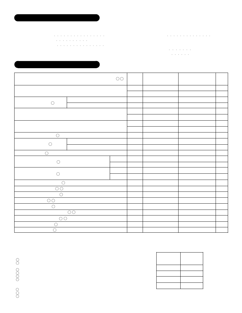
Output Current Limit
Output Noise
Shutdown Output Current
Flag Output Leakage
Flag Output On Voltage
Flag Threshold
Reference Voltage
Reference Voltage Temp Drift
Adjust Pin Bias Current
Thermal Resistance
Thermal Shutdown
Max.
±1.0
±2.0
200
600
±1.0
±2.0
±0.5
±1.0
3.5
20
-
-
-
0.8
75
2
20
2
0.4
-
1.26
-
120
2.6
-
Output Voltage Tolerance
Dropout Voltage
Load Regulation
Line Regulation
Ground Current
Enable Input Voltage
Enable Input Current
Storage Temperature Range
Lead Temperature
(10 Seconds Soldering)
Operating Temperature
MSK 5115 Series
MSK 5115B Series
%
%
mV
mV
%
%
%
%
A
mA
mA
μV
V
V
μA
μA
μA
μA
V
mV
V
ppm
/°C
nA
°C/W
°C
V
OUT
=-1%; I
OUT
=
100m
A
V
OUT
=-1%; I
OUT
=1.5A
V
IN
=V
OUT
+5V
10mA
≤
I
OUT
≤
1.5A
(V
OUT
+1V)
≤
V
IN
≤
26V
I
OUT
=10mA
V
OUT
=0V; V
IN
=V
OUT
+1V
V
IN
=V
OUT
+1V; I
OUT
=0.75A
V
IN
=V
OUT
+1V; I
OUT
=1.5A
C
L
=10μF; 10Hz
≤
f
≤
100KHz
V
ENABLE
≤
0.8V
V
OH
=26V
I
OL
≤
250μA; V
IN
=V
OUT
-2V
V
IN
=V
OUT
-7%
Normal Operation
Normal Operation
Full Temp; V
IN
=V
OUT
+1V
Junction to Case
T
J
Input Voltage (100mS 1%D.C.)
Input Voltage
Enable Voltage
Output Current
Adjustable
+3.3V
+5.0V
+12.0V
V
INP
V
IN
V
EN
I
OUT
Parameter
T
ST
T
LD
T
J
ELECTRICAL SPECIFICATIONS
ABSOLUTE MAXIMUM RATINGS
○
○
○
○
○
○
○
○
○
○
○
○
○
○
○
○
○
○
○
○
○
○
○
○
○
○
○
-65°C to +150°C
300°C
-40°C to +85°C
-55°C to +125°C
1
Test Conditions
1
2
3
4
5
6
7
8
9
NOTES:
Output decoupled to ground using 20μF minimum capacitor unless otherwise specified.
This parameter is guaranteed by design but need not be tested.
Typical parameters are representative of actual device performance but are for reference only.
All output parameters are tested using a low duty cycle pulse to maintain T
J
= T
C
.
Industrial grade devices shall be tested to subgroup 1 unless otherwise specified.
Military grade devices ('B' suffix) shall be 100% tested to subgroups 1,2,3.
Subgroup 1
Subgroup 2
Subgroup 3
Please consult the factory if alternate output voltages are required.
Applies to MSK5115-00 adjustable version only.
Applies to fixed output devices only.
PART
NUMBER
OUTPUT
VOLTAGE
T
C
=+25°C
T
J
=+125°C
T
A
=-55°C
MSK5115-00
MSK5115-3.3
MSK5115-5.0
MSK5115-12
○
○
○
○
○
○
○
○
○
○
○
○
○
○
○
○
○
○
○
○
○
○
○
○
○
○
○
○
○
○
○
○
○
○
○
○
○
○
○
○
○
HIGH/ON
LOW/OFF
HIGH/ON
LOW/OFF
MSK 5115B SERIES
Min.
-
-
-
-
-
-
-
-
-
-
-
-
2.4
-
-
-
-
-
-
-
1.22
-
-
-
-
Typ.
±0.5
±1.0
80
350
±0.2
±0.3
±0.05
±0.5
2.1
8
22
400
1.2
1.2
20
1
10
0.01
0.2
75
1.24
20
40
2.4
130
Typ.
±0.5
-
80
350
±0.2
±0.3
±0.05
±0.5
2.1
8
22
400
1.2
1.2
20
1
10
0.01
0.2
75
1.24
20
40
2.4
130
MSK 5115 SERIES
Min.
-
-
-
-
-
-
-
-
-
-
-
-
2.4
-
-
-
-
-
-
-
1.22
-
-
-
-
Max.
±1.0
-
225
625
±1.2
-
±0.6
-
3.5
20
-
-
-
0.8
75
2
20
2
0.4
-
1.26
-
150
2.7
-
Units
2
2
2
8
2
8
8
2
9
9
2
9
2
3
Group A
Subgroup
1
2,3
1
1
1
2,3
1
2,3
-
-
-
-
1
1
1
1
-
-
1
-
1
-
-
-
-
2
I
OUT
=1A; V
IN
=V
OUT
+1V
2
-20V to +60V
26V
-0.3V to 26V
3.5A
2
2
2
2
2
Rev. B 7/00
相關(guān)PDF資料 |
PDF描述 |
|---|---|
| MSK5115-5.0BZD | HIGH CURRENT, LOW DROPOUT VOLTAGE REGULATORS |
| MSK5115-5.0TD | HIGH CURRENT, LOW DROPOUT VOLTAGE REGULATORS |
| MSK5115-12TU | HIGH CURRENT, LOW DROPOUT VOLTAGE REGULATORS |
| MSK5115-12ZD | HIGH CURRENT, LOW DROPOUT VOLTAGE REGULATORS |
| MSK5115-12ZS | HIGH CURRENT, LOW DROPOUT VOLTAGE REGULATORS |
相關(guān)代理商/技術(shù)參數(shù) |
參數(shù)描述 |
|---|---|
| MSK5116-1.5ETD | 制造商:MSK 制造商全稱:M.S. Kennedy Corporation 功能描述:HIGH CURRENT, LOW DROPOUT VOLTAGE REGULATORS |
| MSK5116-1.5ETS | 制造商:MSK 制造商全稱:M.S. Kennedy Corporation 功能描述:HIGH CURRENT, LOW DROPOUT VOLTAGE REGULATORS |
| MSK5116-1.5ETU | 制造商:MSK 制造商全稱:M.S. Kennedy Corporation 功能描述:HIGH CURRENT, LOW DROPOUT VOLTAGE REGULATORS |
| MSK5116-1.5EZD | 制造商:MSK 制造商全稱:M.S. Kennedy Corporation 功能描述:HIGH CURRENT, LOW DROPOUT VOLTAGE REGULATORS |
| MSK5116-1.5EZS | 制造商:MSK 制造商全稱:M.S. Kennedy Corporation 功能描述:HIGH CURRENT, LOW DROPOUT VOLTAGE REGULATORS |
發(fā)布緊急采購(gòu),3分鐘左右您將得到回復(fù)。