- 您現(xiàn)在的位置:買賣IC網(wǎng) > PDF目錄25627 > MR83C154XXX-16P883D (ATMEL CORP) 8-BIT, MROM, 16 MHz, MICROCONTROLLER, CQCC44 PDF資料下載
參數(shù)資料
| 型號: | MR83C154XXX-16P883D |
| 廠商: | ATMEL CORP |
| 元件分類: | 微控制器/微處理器 |
| 英文描述: | 8-BIT, MROM, 16 MHz, MICROCONTROLLER, CQCC44 |
| 封裝: | LCC-44 |
| 文件頁數(shù): | 20/28頁 |
| 文件大小: | 6193K |
| 代理商: | MR83C154XXX-16P883D |
第1頁第2頁第3頁第4頁第5頁第6頁第7頁第8頁第9頁第10頁第11頁第12頁第13頁第14頁第15頁第16頁第17頁第18頁第19頁當前第20頁第21頁第22頁第23頁第24頁第25頁第26頁第27頁第28頁
27
2467X–AVR–06/11
ATmega128
The control bits for the External Memory Interface are located in three registers, the MCU Con-
trol Register – MCUCR, the External Memory Control Register A – XMCRA, and the External
Memory Control Register B – XMCRB.
When the XMEM interface is enabled, the XMEM interface will override the setting in the data
direction registers that corresponds to the ports dedicated to the XMEM interface. For details
about the port override, see the alternate functions in section “I/O Ports” on page 65. The XMEM
interface will auto-detect whether an access is internal or external. If the access is external, the
XMEM interface will output address, data, and the control signals on the ports according to Fig-
ure 13 (this figure shows the wave forms without wait-states). When ALE goes from high-to-low,
there is a valid address on AD7:0. ALE is low during a data transfer. When the XMEM interface
is enabled, also an internal access will cause activity on address, data and ALE ports, but the
RD and WR strobes will not toggle during internal access. When the External Memory Interface
is disabled, the normal pin and data direction settings are used. Note that when the XMEM inter-
face is disabled, the address space above the internal SRAM boundary is not mapped into the
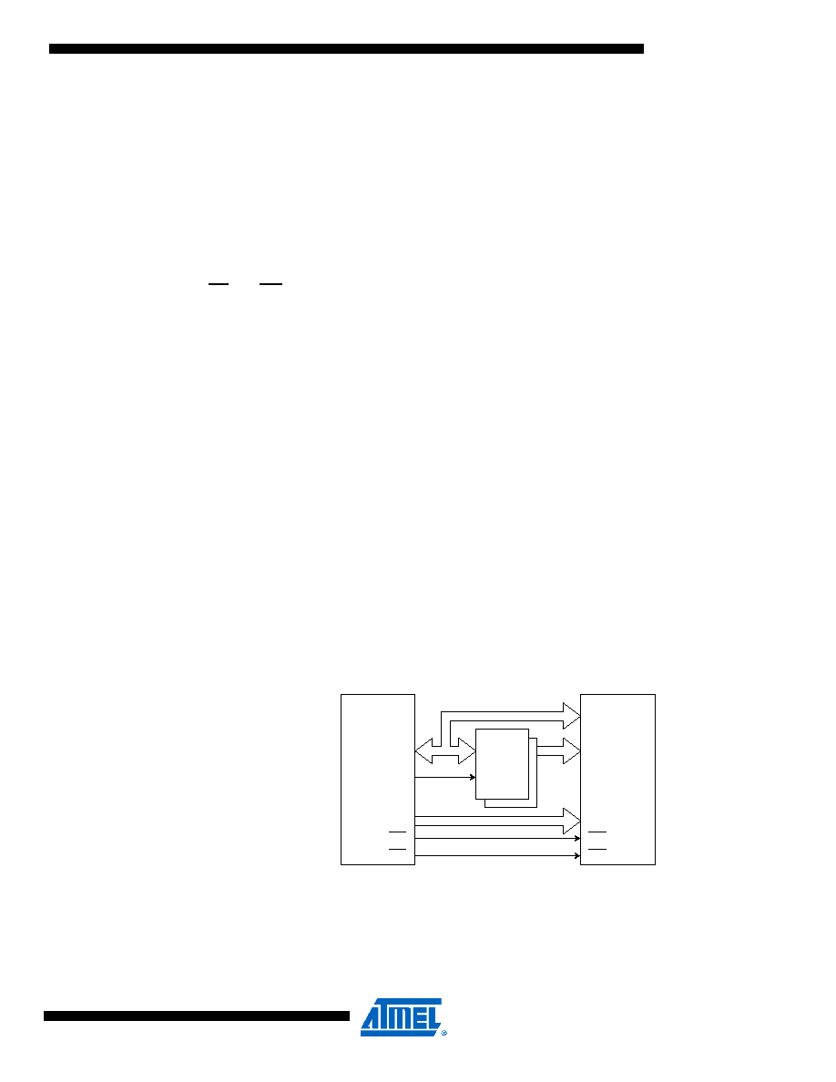
internal SRAM. Figure 12 illustrates how to connect an external SRAM to the AVR using an octal
latch (typically “74 x 573” or equivalent) which is transparent when G is high.
Address Latch
Requirements
Due to the high-speed operation of the XRAM interface, the address latch must be selected with
care for system frequencies above 8MHz @ 4V and 4MHz @ 2.7V. When operating at condi-
tions above these frequencies, the typical old style 74HC series latch becomes inadequate. The
External Memory Interface is designed in compliance to the 74AHC series latch. However, most
latches can be used as long they comply with the main timing parameters. The main parameters
for the address latch are:
D to Q propagation delay (t
PD).
Data setup time before G low (t
SU).
Data (address) hold time after G low (
TH).
The External Memory Interface is designed to guaranty minimum address hold time after G is
asserted low of t
PD) must be taken
into consideration when calculating the access time requirement of the external component. The
data setup time before G low (t
SU) must not exceed address valid to ALE low (tAVLLC) minus PCB
wiring delay (dependent on the capacitive load).
Figure 12. External SRAM Connected to the AVR
D[7:0]
A[7:0]
A[15:8]
RD
WR
SRAM
DQ
G
AD7:0
ALE
A15:8
RD
WR
AVR
相關(guān)PDF資料 |
PDF描述 |
|---|---|
| MR80C52XXX-30/883:RD | 8-BIT, MROM, 30 MHz, MICROCONTROLLER, CQCC44 |
| MQ80C32-36/883R | 8-BIT, 36 MHz, MICROCONTROLLER, CQFP44 |
| MD83C154DXXX-12/883 | 8-BIT, MROM, 12 MHz, MICROCONTROLLER, CDIP40 |
| MF280C51-30D | 8-BIT, MROM, 30 MHz, MICROCONTROLLER, PQFP44 |
| MR80C32E-16P883 | 8-BIT, 16 MHz, MICROCONTROLLER, CQCC44 |
相關(guān)代理商/技術(shù)參數(shù) |
參數(shù)描述 |
|---|---|
| MR850 | 功能描述:整流器 3.0 Amp 50 Volt 150ns RoHS:否 制造商:Vishay Semiconductors 產(chǎn)品:Standard Recovery Rectifiers 配置: 反向電壓:100 V 正向電壓下降: 恢復時間:1.2 us 正向連續(xù)電流:2 A 最大浪涌電流:35 A 反向電流 IR:5 uA 安裝風格:SMD/SMT 封裝 / 箱體:DO-221AC 封裝:Reel |
| MR850 _AY _10001 | 制造商:PanJit Touch Screens 功能描述: |
| MR850 R0 | 制造商:SKMI/Taiwan 功能描述:Diode Switching 50V 3A 2-Pin DO-201AD T/R |
| MR850_ R2 _10001 | 制造商:PanJit Touch Screens 功能描述: |
| MR850_09 | 制造商:PANJIT 制造商全稱:Pan Jit International Inc. 功能描述:SOFT RECOVERY, FAST SWITCHING PLASTIC RECTIFIER |
發(fā)布緊急采購,3分鐘左右您將得到回復。