- 您現(xiàn)在的位置:買賣IC網(wǎng) > PDF目錄25640 > MR80C52EXXX-16SHXXX:R (ATMEL CORP) 8-BIT, MROM, 16 MHz, MICROCONTROLLER, CQCC44 PDF資料下載
參數(shù)資料
| 型號: | MR80C52EXXX-16SHXXX:R |
| 廠商: | ATMEL CORP |
| 元件分類: | 微控制器/微處理器 |
| 英文描述: | 8-BIT, MROM, 16 MHz, MICROCONTROLLER, CQCC44 |
| 封裝: | LCC-44 |
| 文件頁數(shù): | 35/143頁 |
| 文件大小: | 4602K |
第1頁第2頁第3頁第4頁第5頁第6頁第7頁第8頁第9頁第10頁第11頁第12頁第13頁第14頁第15頁第16頁第17頁第18頁第19頁第20頁第21頁第22頁第23頁第24頁第25頁第26頁第27頁第28頁第29頁第30頁第31頁第32頁第33頁第34頁當前第35頁第36頁第37頁第38頁第39頁第40頁第41頁第42頁第43頁第44頁第45頁第46頁第47頁第48頁第49頁第50頁第51頁第52頁第53頁第54頁第55頁第56頁第57頁第58頁第59頁第60頁第61頁第62頁第63頁第64頁第65頁第66頁第67頁第68頁第69頁第70頁第71頁第72頁第73頁第74頁第75頁第76頁第77頁第78頁第79頁第80頁第81頁第82頁第83頁第84頁第85頁第86頁第87頁第88頁第89頁第90頁第91頁第92頁第93頁第94頁第95頁第96頁第97頁第98頁第99頁第100頁第101頁第102頁第103頁第104頁第105頁第106頁第107頁第108頁第109頁第110頁第111頁第112頁第113頁第114頁第115頁第116頁第117頁第118頁第119頁第120頁第121頁第122頁第123頁第124頁第125頁第126頁第127頁第128頁第129頁第130頁第131頁第132頁第133頁第134頁第135頁第136頁第137頁第138頁第139頁第140頁第141頁第142頁第143頁
13
XMEGA A3BU [DATASHEET]
8362F–AVR–02/2013
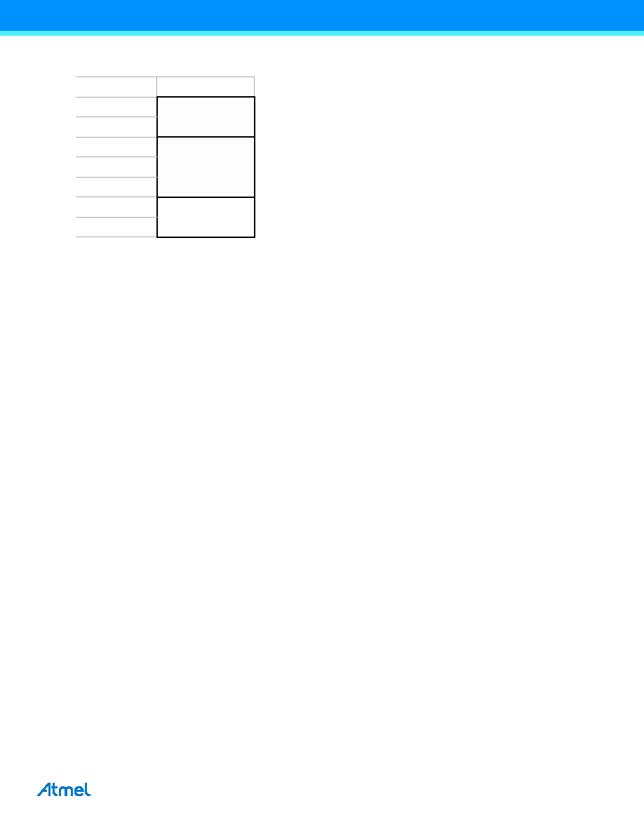
Figure 7-2.
Data memory map (Hexadecimal address).
7.6
EEPROM
XMEGA AU devices have EEPROM for nonvolatile data storage. It is either addressable in a separate data space
(default) or memory mapped and accessed in normal data space. The EEPROM supports both byte and page access.
Memory mapped EEPROM allows highly efficient EEPROM reading and EEPROM buffer loading. When doing this,
EEPROM is accessible using load and store instructions. Memory mapped EEPROM will always start at hexadecimal
address 0x1000.
7.7
I/O Memory
The status and configuration registers for peripherals and modules, including the CPU, are addressable through I/O
memory locations. All I/O locations can be accessed by the load (LD/LDS/LDD) and store (ST/STS/STD) instructions,
which are used to transfer data between the 32 registers in the register file and the I/O memory. The IN and OUT
instructions can address I/O memory locations in the range of 0x00 to 0x3F directly. In the address range 0x00 - 0x1F,
single-cycle instructions for manipulation and checking of individual bits are available.
The I/O memory address for all peripherals and modules in XMEGA A3BU is shown in the “Peripheral Module Address
7.7.1
General Purpose I/O Registers
The lowest 16 I/O memory addresses are reserved as general purpose I/O registers. These registers can be used for
storing global variables and flags, as they are directly bit-accessible using the SBI, CBI, SBIS, and SBIC instructions.
7.8
Data Memory and Bus Arbitration
Since the data memory is organized as four separate sets of memories, the different bus masters (CPU, DMA controller
read and DMA controller write, etc.) can access different memory sections at the same time.
7.9
Memory Timing
Read and write access to the I/O memory takes one CPU clock cycle. A write to SRAM takes one cycle, and a read from
SRAM takes two cycles. For burst read (DMA), new data are available every cycle. EEPROM page load (write) takes one
cycle, and three cycles are required for read. For burst read, new data are available every second cycle. Refer to the
instruction summary for more details on instructions and instruction timing.
7.10
Device ID and Revision
Each device has a three-byte device ID. This ID identifies Atmel as the manufacturer of the device and the device type. A
separate register contains the revision number of the device.
Byte Address
ATxmega256A3BU
0
I/O Registers
(4K)
FFF
1000
EEPROM
(4K)
1FFF
2000
Internal SRAM
(16K)
5FFF
相關PDF資料 |
PDF描述 |
|---|---|
| MD83C154DCXXX-25P883D | 8-BIT, MROM, 25 MHz, MICROCONTROLLER, CDIP40 |
| S80C32E-20R | 8-BIT, 20 MHz, MICROCONTROLLER, PQCC44 |
| MQ83C154CXXX-12P883R | 8-BIT, MROM, 12 MHz, MICROCONTROLLER, CQFP44 |
| MC80C52EXXX-25SHXXX | 8-BIT, MROM, 25 MHz, MICROCONTROLLER, CDIP40 |
| MC80C52XXX-30/883:D | 8-BIT, MROM, 30 MHz, MICROCONTROLLER, CDIP40 |
相關代理商/技術參數(shù) |
參數(shù)描述 |
|---|---|
| MR80C86 | 制造商:INTERSIL 制造商全稱:Intersil Corporation 功能描述:CMOS 16-Bit Microprocessor |
| MR80C86/B | 制造商:Rochester Electronics LLC 功能描述:- Bulk 制造商:Harris Corporation 功能描述:Microprocessor, 16 Bit, 44 Pin, Ceramic, LCC |
| MR80C86-2 | 制造商:INTERSIL 制造商全稱:Intersil Corporation 功能描述:CMOS 16-Bit Microprocessor |
| MR80C86-2/883 | 制造商:Rochester Electronics LLC 功能描述:- Bulk |
| MR80C86-2/B | 制造商:Intersil Corporation 功能描述:MPU 80C86 16BIT CMOS 8MHZ 44PLCC - Rail/Tube |
發(fā)布緊急采購,3分鐘左右您將得到回復。