- 您現(xiàn)在的位置:買賣IC網(wǎng) > PDF目錄45381 > MQ83C154DTXXX-12/883 (ATMEL CORP) 8-BIT, MROM, 12 MHz, MICROCONTROLLER, CQFP44 PDF資料下載
參數(shù)資料
| 型號: | MQ83C154DTXXX-12/883 |
| 廠商: | ATMEL CORP |
| 元件分類: | 微控制器/微處理器 |
| 英文描述: | 8-BIT, MROM, 12 MHz, MICROCONTROLLER, CQFP44 |
| 封裝: | CERAMIC, QFP-44 |
| 文件頁數(shù): | 83/242頁 |
| 文件大?。?/td> | 3080K |
| 代理商: | MQ83C154DTXXX-12/883 |
第1頁第2頁第3頁第4頁第5頁第6頁第7頁第8頁第9頁第10頁第11頁第12頁第13頁第14頁第15頁第16頁第17頁第18頁第19頁第20頁第21頁第22頁第23頁第24頁第25頁第26頁第27頁第28頁第29頁第30頁第31頁第32頁第33頁第34頁第35頁第36頁第37頁第38頁第39頁第40頁第41頁第42頁第43頁第44頁第45頁第46頁第47頁第48頁第49頁第50頁第51頁第52頁第53頁第54頁第55頁第56頁第57頁第58頁第59頁第60頁第61頁第62頁第63頁第64頁第65頁第66頁第67頁第68頁第69頁第70頁第71頁第72頁第73頁第74頁第75頁第76頁第77頁第78頁第79頁第80頁第81頁第82頁當前第83頁第84頁第85頁第86頁第87頁第88頁第89頁第90頁第91頁第92頁第93頁第94頁第95頁第96頁第97頁第98頁第99頁第100頁第101頁第102頁第103頁第104頁第105頁第106頁第107頁第108頁第109頁第110頁第111頁第112頁第113頁第114頁第115頁第116頁第117頁第118頁第119頁第120頁第121頁第122頁第123頁第124頁第125頁第126頁第127頁第128頁第129頁第130頁第131頁第132頁第133頁第134頁第135頁第136頁第137頁第138頁第139頁第140頁第141頁第142頁第143頁第144頁第145頁第146頁第147頁第148頁第149頁第150頁第151頁第152頁第153頁第154頁第155頁第156頁第157頁第158頁第159頁第160頁第161頁第162頁第163頁第164頁第165頁第166頁第167頁第168頁第169頁第170頁第171頁第172頁第173頁第174頁第175頁第176頁第177頁第178頁第179頁第180頁第181頁第182頁第183頁第184頁第185頁第186頁第187頁第188頁第189頁第190頁第191頁第192頁第193頁第194頁第195頁第196頁第197頁第198頁第199頁第200頁第201頁第202頁第203頁第204頁第205頁第206頁第207頁第208頁第209頁第210頁第211頁第212頁第213頁第214頁第215頁第216頁第217頁第218頁第219頁第220頁第221頁第222頁第223頁第224頁第225頁第226頁第227頁第228頁第229頁第230頁第231頁第232頁第233頁第234頁第235頁第236頁第237頁第238頁第239頁第240頁第241頁第242頁
173
2588F–AVR–06/2013
ATtiny261/461/861
18.4
Calibration Byte
Signature area of the ATtiny261/461/861 has one byte of calibration data for the internal RC
Oscillator. This byte resides in the high byte of address 0x000. During reset, this byte is auto-
matically written into the OSCCAL Register to ensure correct frequency of the calibrated RC
Oscillator.
18.5
Page Size
18.6
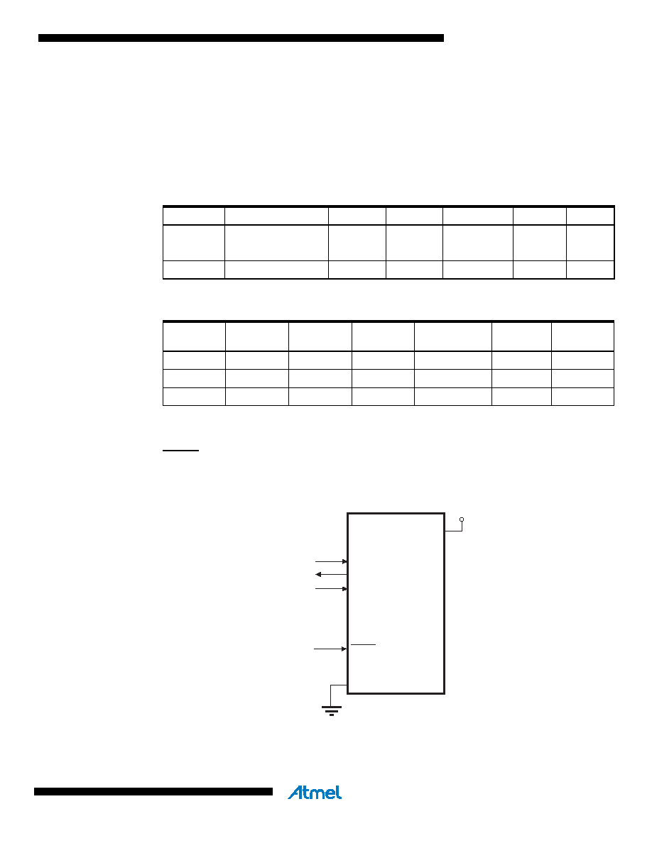
Serial Programming
Both the Flash and EEPROM memory arrays can be programmed using the serial SPI bus while
RESET is pulled to GND. The serial interface consists of pins SCK, MOSI (input) and MISO (out-
put). See Figure 18-1.
Figure 18-1. Serial Programming and Verify
Note:
If the device is clocked by the internal Oscillator, there is no need to connect a clock source to the
CLKI pin.
Table 18-7.
No. of Words in a Page and No. of Pages in the Flash
Device
Flash Size
Page Size
PCWORD
No. of Pages
PCPAGE
PCMSB
ATtiny261
1K words (2K bytes)
16 words
PC[3:0]
64
PC[9:4]
9
ATtiny461
2K words (4K bytes)
32 words
PC[4:0]
64
PC[10:5]
10
ATtiny861
4K words (8K bytes)
32 words
PC[4:0]
128
PC[11:5]
11
Table 18-8.
No. of Words in a Page and No. of Pages in the EEPROM
Device
EEPROM
Size
Page Size
PCWORD
No. of Pages
PCPAGE
EEAMSB
ATtiny261
128 bytes
4 bytes
EEA[1:0]
32
EEA[6:2]
6
ATtiny461
256 bytes
4 bytes
EEA[1:0]
64
EEA[7:2]
7
ATtiny861
512 bytes
4 bytes
EEA[1:0]
128
EEA[8:2]
8
VCC
GND
SCK
MISO
MOSI
RESET
+1.8 - 5.5V
發(fā)布緊急采購,3分鐘左右您將得到回復。