- 您現(xiàn)在的位置:買賣IC網(wǎng) > PDF目錄98034 > MPSH81RLRM (ON SEMICONDUCTOR) Si, PNP, RF SMALL SIGNAL TRANSISTOR, TO-92 PDF資料下載
參數(shù)資料
| 型號(hào): | MPSH81RLRM |
| 廠商: | ON SEMICONDUCTOR |
| 元件分類: | 小信號(hào)晶體管 |
| 英文描述: | Si, PNP, RF SMALL SIGNAL TRANSISTOR, TO-92 |
| 封裝: | PLASTIC, TO-226AA, 3 PIN |
| 文件頁數(shù): | 1/35頁 |
| 文件大?。?/td> | 320K |
| 代理商: | MPSH81RLRM |
當(dāng)前第1頁第2頁第3頁第4頁第5頁第6頁第7頁第8頁第9頁第10頁第11頁第12頁第13頁第14頁第15頁第16頁第17頁第18頁第19頁第20頁第21頁第22頁第23頁第24頁第25頁第26頁第27頁第28頁第29頁第30頁第31頁第32頁第33頁第34頁第35頁
2–673
Motorola Small–Signal Transistors, FETs and Diodes Device Data
RF Amplifier Transistor
PNP Silicon
MAXIMUM RATINGS
Rating
Symbol
Value
Unit
Collector – Emitter Voltage
VCEO
–20
Vdc
Collector – Base Voltage
VCBO
–20
Vdc
Emitter – Base Voltage
VEBO
–3.0
Vdc
Total Device Dissipation @ TA = 25°C
Derate above 25
°C
PD
350
2.81
mW
mW/
°C
Operating and Storage Junction
Temperature Range
TJ, Tstg
– 55 to +150
°C
THERMAL CHARACTERISTICS
Characteristic
Symbol
Max
Unit
Thermal Resistance, Junction to Ambient
RqJA
357
°C/W
ELECTRICAL CHARACTERISTICS (TA = 25°C unless otherwise noted)
Characteristic
Symbol
Min
Typ
Max
Unit
OFF CHARACTERISTICS
Collector – Emitter Breakdown Voltage
(IC = –1.0 mAdc, IB = 0)
V(BR)CEO
–20
—
Vdc
Collector – Base Breakdown Voltage
(IC = –10 mAdc, IE = 0)
V(BR)CBO
–20
—
Vdc
Emitter – Base Breakdown Voltage
(IE = –10 mAdc, IC = 0)
V(BR)EBO
–3.0
—
Vdc
Collector Cutoff Current
(VCB = –10 Vdc, IE = 0)
ICBO
—
–100
nAdc
Emitter Cutoff Current
(VEB = –2.0 Vdc, IC = 0)
IEBO
—
–100
nAdc
Preferred devices are Motorola recommended choices for future use and best overall value.
MOTOROLA
SEMICONDUCTOR TECHNICAL DATA
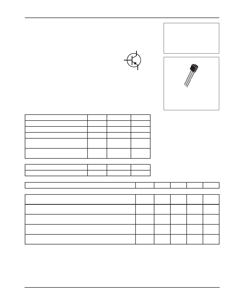
MPSH81
Motorola Preferred Device
CASE 29–04, STYLE 2
TO–92 (TO–226AA)
1
2
3
COLLECTOR
3
1
BASE
2
EMITTER
相關(guān)PDF資料 |
PDF描述 |
|---|---|
| MPSH81RL | Si, PNP, RF SMALL SIGNAL TRANSISTOR, TO-92 |
| MPSH81RLRA | Si, PNP, RF SMALL SIGNAL TRANSISTOR, TO-92 |
| MPSH81RLRE | Si, PNP, RF SMALL SIGNAL TRANSISTOR, TO-92 |
| MPSH81 | Si, PNP, RF SMALL SIGNAL TRANSISTOR, TO-92 |
| MPSL01ZL1 | 150 mA, 120 V, NPN, Si, SMALL SIGNAL TRANSISTOR, TO-92 |
相關(guān)代理商/技術(shù)參數(shù) |
參數(shù)描述 |
|---|---|
| MPSH8-D20-120V | 制造商:Black Box Corporation 功能描述:8 OUTLET 120V 20A DUAL CIRCUIT OUTLET METERING |
| MPSH8-D20-120V-W1 | 制造商:Black Box Corporation 功能描述:1 YEAR WARRANTY FOR MPSH8-D20-120V |
| MPSH8-D20-120V-W3 | 制造商:Black Box Corporation 功能描述:3 YEAR WARRANTY FOR MPSH8-D20-120V |
| MPSH8-D20-208+V | 制造商:Black Box Corporation 功能描述:8 OUTLET 208+V 20A DUAL CIRCUIT OUTLET METERING |
| MPSH8-D20-208+VT | 制造商:Black Box Corporation 功能描述:8 OUTLET 208+V 20A DUAL CIRCUIT OUTLET METERING |
發(fā)布緊急采購,3分鐘左右您將得到回復(fù)。