- 您現(xiàn)在的位置:買賣IC網(wǎng) > PDF目錄4040 > MPC8572VTAULE (Freescale Semiconductor)MPU POWERQUICC III 1023FCPBGA PDF資料下載
參數(shù)資料
| 型號: | MPC8572VTAULE |
| 廠商: | Freescale Semiconductor |
| 文件頁數(shù): | 120/138頁 |
| 文件大?。?/td> | 0K |
| 描述: | MPU POWERQUICC III 1023FCPBGA |
| 標(biāo)準(zhǔn)包裝: | 1 |
| 系列: | MPC85xx |
| 處理器類型: | 32-位 MPC85xx PowerQUICC III |
| 速度: | 1.333GHz |
| 電壓: | 1.1V |
| 安裝類型: | 表面貼裝 |
| 封裝/外殼: | 1023-BBGA,F(xiàn)CBGA |
| 供應(yīng)商設(shè)備封裝: | 1023-FCPBGA(33x33) |
| 包裝: | 托盤 |
第1頁第2頁第3頁第4頁第5頁第6頁第7頁第8頁第9頁第10頁第11頁第12頁第13頁第14頁第15頁第16頁第17頁第18頁第19頁第20頁第21頁第22頁第23頁第24頁第25頁第26頁第27頁第28頁第29頁第30頁第31頁第32頁第33頁第34頁第35頁第36頁第37頁第38頁第39頁第40頁第41頁第42頁第43頁第44頁第45頁第46頁第47頁第48頁第49頁第50頁第51頁第52頁第53頁第54頁第55頁第56頁第57頁第58頁第59頁第60頁第61頁第62頁第63頁第64頁第65頁第66頁第67頁第68頁第69頁第70頁第71頁第72頁第73頁第74頁第75頁第76頁第77頁第78頁第79頁第80頁第81頁第82頁第83頁第84頁第85頁第86頁第87頁第88頁第89頁第90頁第91頁第92頁第93頁第94頁第95頁第96頁第97頁第98頁第99頁第100頁第101頁第102頁第103頁第104頁第105頁第106頁第107頁第108頁第109頁第110頁第111頁第112頁第113頁第114頁第115頁第116頁第117頁第118頁第119頁當(dāng)前第120頁第121頁第122頁第123頁第124頁第125頁第126頁第127頁第128頁第129頁第130頁第131頁第132頁第133頁第134頁第135頁第136頁第137頁第138頁
MPC8572E PowerQUICC III Integrated Processor Hardware Specifications, Rev. 5
82
Freescale Semiconductor
PCI Express
16.1
DC Requirements for PCI Express SD1_REF_CLK and
SD1_REF_CLK
For more information, see Section 15.2, “SerDes Reference Clocks.”
16.2
AC Requirements for PCI Express SerDes Reference Clocks
Table 61 lists AC requirements.
16.3
Clocking Dependencies
The ports on the two ends of a link must transmit data at a rate that is within 600 parts per million (ppm)
of each other at all times. This is specified to allow bit rate clock sources with a +/– 300 ppm tolerance.
16.4
Physical Layer Specifications
The following is a summary of the specifications for the physical layer of PCI Express on this device. For
further details as well as the specifications of the transport and data link layer, Use the PCI Express Base
Specification. REV. 1.0a document.
16.4.1
Differential Transmitter (TX) Output
Table 62 defines the specifications for the differential output at all transmitters (TXs). The parameters are
specified at the component pins.
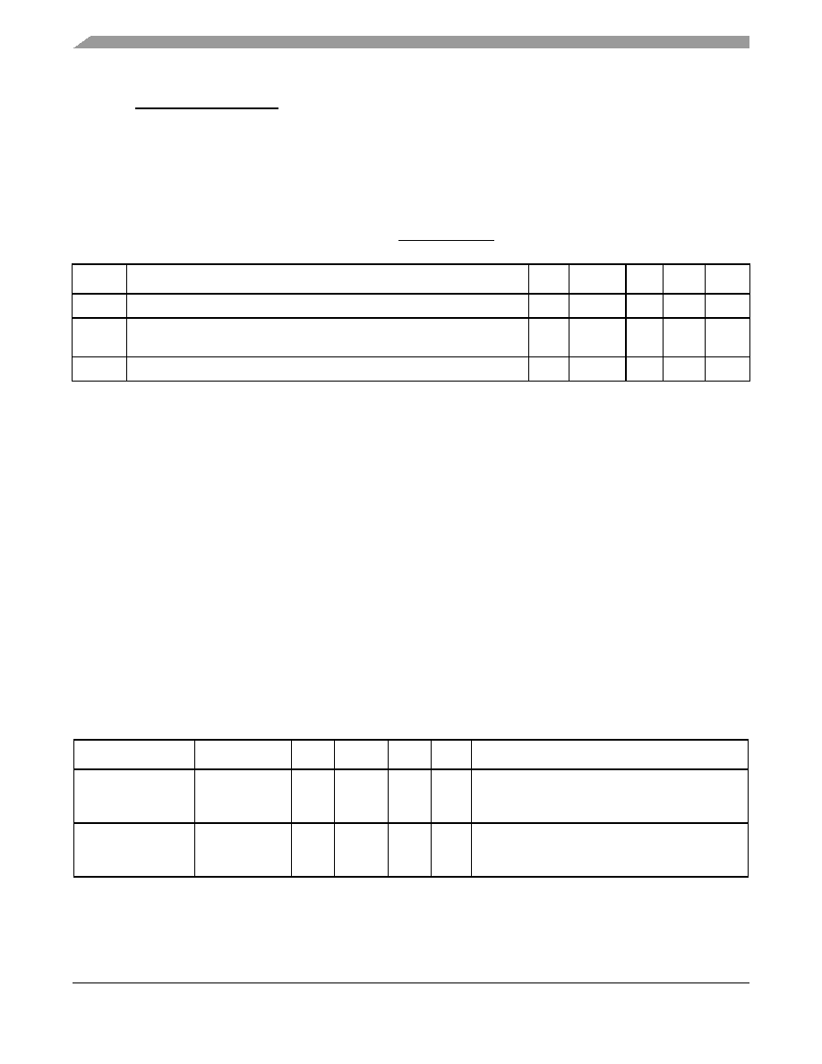
Table 61. SD1_REF_CLK and SD1_REF_CLK AC Requirements
Symbol
Parameter Description
Min
Typical
Max
Units
Notes
tREF
REFCLK cycle time
—
10
—
ns
1
tREFCJ
REFCLK cycle-to-cycle jitter. Difference in the period of any two adjacent
REFCLK cycles
—
100
ps
—
tREFPJ
Phase jitter. Deviation in edge location with respect to mean edge location
–50
—
50
ps
—
Notes:
1. Typical cycle time is based on PCI Express Card Electromechanical Specification Revision 1.0a.
Table 62. Differential Transmitter (TX) Output Specifications
Symbol
Parameter
Min
Nominal
Max
Units
Comments
UI
Unit Interval
399.88
400
400.12
ps
Each UI is 400 ps ± 300 ppm. UI does not account
for Spread Spectrum Clock dictated variations. See
Note 1.
VTX-DIFFp-p
Differential
Peak-to-Peak
Output Voltage
0.8
—
1.2
V
VTX-DIFFp-p = 2*|VTX-D+ - VTX-D-| See Note 2.
發(fā)布緊急采購,3分鐘左右您將得到回復(fù)。