- 您現(xiàn)在的位置:買賣IC網(wǎng) > PDF目錄3937 > MPC8572PXAULD (Freescale Semiconductor)MPU POWERQUICC III 1023-PBGA PDF資料下載
參數(shù)資料
| 型號: | MPC8572PXAULD |
| 廠商: | Freescale Semiconductor |
| 文件頁數(shù): | 35/138頁 |
| 文件大?。?/td> | 0K |
| 描述: | MPU POWERQUICC III 1023-PBGA |
| 標(biāo)準(zhǔn)包裝: | 1 |
| 系列: | MPC85xx |
| 處理器類型: | 32-位 MPC85xx PowerQUICC III |
| 速度: | 1.333GHz |
| 電壓: | 1.1V |
| 安裝類型: | 表面貼裝 |
| 封裝/外殼: | 1023-BBGA,F(xiàn)CBGA |
| 供應(yīng)商設(shè)備封裝: | 1023-FCPBGA(33x33) |
| 包裝: | 托盤 |
第1頁第2頁第3頁第4頁第5頁第6頁第7頁第8頁第9頁第10頁第11頁第12頁第13頁第14頁第15頁第16頁第17頁第18頁第19頁第20頁第21頁第22頁第23頁第24頁第25頁第26頁第27頁第28頁第29頁第30頁第31頁第32頁第33頁第34頁當(dāng)前第35頁第36頁第37頁第38頁第39頁第40頁第41頁第42頁第43頁第44頁第45頁第46頁第47頁第48頁第49頁第50頁第51頁第52頁第53頁第54頁第55頁第56頁第57頁第58頁第59頁第60頁第61頁第62頁第63頁第64頁第65頁第66頁第67頁第68頁第69頁第70頁第71頁第72頁第73頁第74頁第75頁第76頁第77頁第78頁第79頁第80頁第81頁第82頁第83頁第84頁第85頁第86頁第87頁第88頁第89頁第90頁第91頁第92頁第93頁第94頁第95頁第96頁第97頁第98頁第99頁第100頁第101頁第102頁第103頁第104頁第105頁第106頁第107頁第108頁第109頁第110頁第111頁第112頁第113頁第114頁第115頁第116頁第117頁第118頁第119頁第120頁第121頁第122頁第123頁第124頁第125頁第126頁第127頁第128頁第129頁第130頁第131頁第132頁第133頁第134頁第135頁第136頁第137頁第138頁
MPC8572E PowerQUICC III Integrated Processor Hardware Specifications, Rev. 5
Freescale Semiconductor
13
Electrical Characteristics
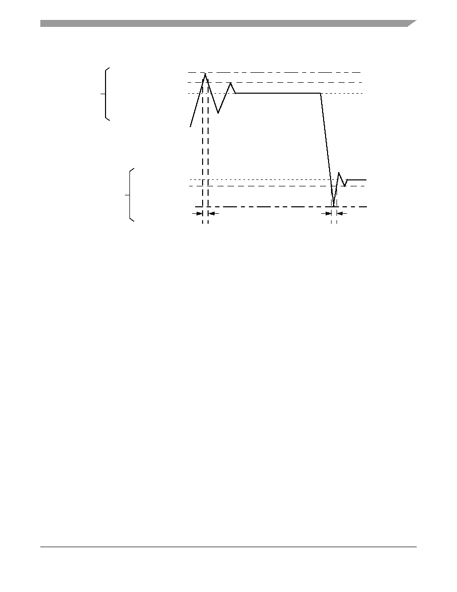
Figure 2 shows the undershoot and overshoot voltages at the interfaces of the MPC8572E.
Figure 2. Overshoot/Undershoot Voltage for TVDD/BVDD/GVDD/LVDD/OVDD
The core voltage must always be provided at nominal 1.1 V. (See Table 2 for actual recommended core
be provided at the voltages shown in Table 2. The input voltage threshold scales with respect to the
associated I/O supply voltage. TVDD, BVDD, OVDD, and LVDD based receivers are simple CMOS I/O
circuits and satisfy appropriate LVCMOS type specifications. The DDR2 and DDR3 SDRAM interface
uses differential receivers referenced by the externally supplied MVREFn signal (nominally set to GVDD/2)
as is appropriate for the SSTL_1.8 electrical signaling standard for DDR2 or 1.5-V electrical signaling for
DDR3. The DDR DQS receivers cannot be operated in single-ended fashion. The complement signal must
be properly driven and cannot be grounded.
GND
GND – 0.3 V
GND – 0.7 V
Not to Exceed 10%
T/B/G/L/OVDD + 20%
T/B/G/L/OVDD
T/B/G/L/OVDD + 5%
of tCLOCK1
tCLOCK refers to the clock period associated with the respective interface:
VIH
VIL
Note:
For I2C and JTAG, tCLOCK references SYSCLK.
For DDR, tCLOCK references MCLK.
For eTSEC, tCLOCK references EC_GTX_CLK125.
For eLBC, tCLOCK references LCLK.
相關(guān)PDF資料 |
PDF描述 |
|---|---|
| MPC8572PXAULB | MPU POWERQUICC III 1023-PBGA |
| MPC8572PXATLD | MPU POWERQUICC III 1023-PBGA |
| MPC8572PXATLB | MPU POWERQUICC III 1023-PBGA |
| MPC8572PXARLD | MPU POWERQUICC III 1023-PBGA |
| MPC8572PXARLB | MPU POWERQUICC III 1023-PBGA |
相關(guān)代理商/技術(shù)參數(shù) |
參數(shù)描述 |
|---|---|
| MPC8572PXAULE | 制造商:Freescale Semiconductor 功能描述:38H R211 NOE SNPB 1333 - Bulk |
| MPC8572PXAVNB | 功能描述:微處理器 - MPU RV1.1.1 SNPB 1500 NOTENC RoHS:否 制造商:Atmel 處理器系列:SAMA5D31 核心:ARM Cortex A5 數(shù)據(jù)總線寬度:32 bit 最大時鐘頻率:536 MHz 程序存儲器大小:32 KB 數(shù)據(jù) RAM 大小:128 KB 接口類型:CAN, Ethernet, LIN, SPI,TWI, UART, USB 工作電源電壓:1.8 V to 3.3 V 最大工作溫度:+ 85 C 安裝風(fēng)格:SMD/SMT 封裝 / 箱體:FBGA-324 |
| MPC8572PXAVND | 功能描述:微處理器 - MPU PQ38H CSM SNPB 1500 RoHS:否 制造商:Atmel 處理器系列:SAMA5D31 核心:ARM Cortex A5 數(shù)據(jù)總線寬度:32 bit 最大時鐘頻率:536 MHz 程序存儲器大小:32 KB 數(shù)據(jù) RAM 大小:128 KB 接口類型:CAN, Ethernet, LIN, SPI,TWI, UART, USB 工作電源電壓:1.8 V to 3.3 V 最大工作溫度:+ 85 C 安裝風(fēng)格:SMD/SMT 封裝 / 箱體:FBGA-324 |
| MPC8572PXAVNE | 制造商:Freescale Semiconductor 功能描述:38H R211 NOE SNPB 1500 - Bulk |
| MPC8572VTARLB | 功能描述:微處理器 - MPU RV1.1.1 1067 NE RoHS:否 制造商:Atmel 處理器系列:SAMA5D31 核心:ARM Cortex A5 數(shù)據(jù)總線寬度:32 bit 最大時鐘頻率:536 MHz 程序存儲器大小:32 KB 數(shù)據(jù) RAM 大小:128 KB 接口類型:CAN, Ethernet, LIN, SPI,TWI, UART, USB 工作電源電壓:1.8 V to 3.3 V 最大工作溫度:+ 85 C 安裝風(fēng)格:SMD/SMT 封裝 / 箱體:FBGA-324 |
發(fā)布緊急采購,3分鐘左右您將得到回復(fù)。