- 您現(xiàn)在的位置:買賣IC網(wǎng) > PDF目錄45373 > MPC8572EPXAVNB (FREESCALE SEMICONDUCTOR INC) 32-BIT, 1500 MHz, MICROPROCESSOR, PBGA1023 PDF資料下載
參數(shù)資料
| 型號(hào): | MPC8572EPXAVNB |
| 廠商: | FREESCALE SEMICONDUCTOR INC |
| 元件分類: | 微控制器/微處理器 |
| 英文描述: | 32-BIT, 1500 MHz, MICROPROCESSOR, PBGA1023 |
| 封裝: | 33 X 33 MM, PLASTIC, FCBGA-1023 |
| 文件頁數(shù): | 71/138頁 |
| 文件大小: | 1502K |
| 代理商: | MPC8572EPXAVNB |
第1頁第2頁第3頁第4頁第5頁第6頁第7頁第8頁第9頁第10頁第11頁第12頁第13頁第14頁第15頁第16頁第17頁第18頁第19頁第20頁第21頁第22頁第23頁第24頁第25頁第26頁第27頁第28頁第29頁第30頁第31頁第32頁第33頁第34頁第35頁第36頁第37頁第38頁第39頁第40頁第41頁第42頁第43頁第44頁第45頁第46頁第47頁第48頁第49頁第50頁第51頁第52頁第53頁第54頁第55頁第56頁第57頁第58頁第59頁第60頁第61頁第62頁第63頁第64頁第65頁第66頁第67頁第68頁第69頁第70頁當(dāng)前第71頁第72頁第73頁第74頁第75頁第76頁第77頁第78頁第79頁第80頁第81頁第82頁第83頁第84頁第85頁第86頁第87頁第88頁第89頁第90頁第91頁第92頁第93頁第94頁第95頁第96頁第97頁第98頁第99頁第100頁第101頁第102頁第103頁第104頁第105頁第106頁第107頁第108頁第109頁第110頁第111頁第112頁第113頁第114頁第115頁第116頁第117頁第118頁第119頁第120頁第121頁第122頁第123頁第124頁第125頁第126頁第127頁第128頁第129頁第130頁第131頁第132頁第133頁第134頁第135頁第136頁第137頁第138頁
MPC8572E PowerQUICC III Integrated Processor Hardware Specifications, Rev. 2
38
Freescale Semiconductor
Ethernet: Enhanced Three-Speed Ethernet (eTSEC)
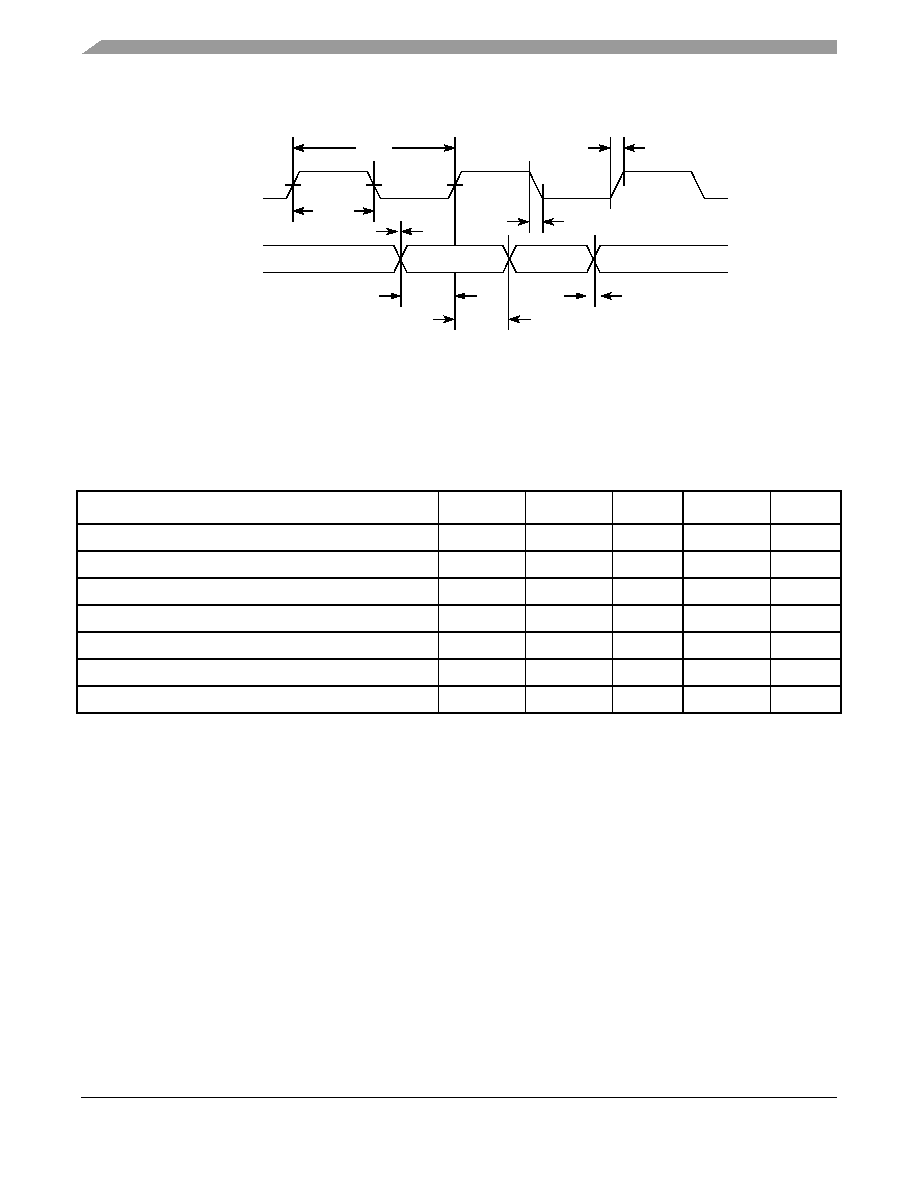
Figure 15 shows the TBI transmit AC timing diagram.
Figure 15. TBI Transmit AC Timing Diagram
8.2.4.2
TBI Receive AC Timing Specifications
Table 31 provides the TBI receive AC timing specifications.
Table 31. TBI Receive AC Timing Specifications
At recommended operating conditions with LVDD/TVDD of 2.5/ 3.3 V ± 5%.
Parameter/Condition 3
Symbol 1
Min
Typ
Max
Unit
Clock period for TBI Receive Clock 0, 1
tTRX
—
16.0
—
ns
Skew for TBI Receive Clock 0, 1
tSKTRX
7.5
—
8.5
ns
Duty cycle for TBI Receive Clock 0, 1
tTRXH/tTRX
40
—
60
%
RCG[9:0] setup time to rising edge of TBI Receive Clock 0, 1
tTRDVKH
2.5
——ns
RCG[9:0] hold time to rising edge of TBI Receive Clock 0, 1
tTRDXKH
1.5
——ns
Clock rise time (20%-80%) for TBI Receive Clock 0, 1
tTRXR
2
0.7
—
2.4
ns
Clock fall time (80%-20%) for TBI Receive Clock 0, 1
tTRXF
2
0.7
—
2.4
ns
Notes:
1. The symbols used for timing specifications herein follow the pattern of t(first two letters of functional block)(signal)(state) (reference)(state)
for inputs and t(first two letters of functional block)(reference)(state)(signal)(state) for outputs. For example, tTRDVKH symbolizes TBI receive
timing (TR) with respect to the time data input signals (D) reach the valid state (V) relative to the tTRX clock reference (K) going
to the high (H) state or setup time. Also, tTRDXKH symbolizes TBI receive timing (TR) with respect to the time data input signals
(D) went invalid (X) relative to the tTRX clock reference (K) going to the high (H) state. Note that, in general, the clock reference
symbol representation is based on three letters representing the clock of a particular functional. For example, the subscript of
tTRX represents the TBI (T) receive (RX) clock. For rise and fall times, the latter convention is used with the appropriate letter:
R (rise) or F (fall). For symbols representing skews, the subscript is skew (SK) followed by the clock that is being skewed
(TRX).
2. Guaranteed by design.
3. The signals “TBI Receive Clock 0” and “TBI Receive Clock 1” refer to TSECn_RX_CLK and TSECn_TX_CLK pins
respectively. These two clock signals are also referred as PMA_RX_CLK[0:1].
GTX_CLK
TCG[9:0]
tTTXR
tTTX
tTTXH
tTTXR
tTTXF
tTTKHDV
tTTKHDX
tTTXF
發(fā)布緊急采購,3分鐘左右您將得到回復(fù)。