- 您現(xiàn)在的位置:買賣IC網(wǎng) > PDF目錄3938 > MPC8572ECPXAULB (Freescale Semiconductor)MPU POWERQUICC III 1023-PBGA PDF資料下載
參數(shù)資料
| 型號: | MPC8572ECPXAULB |
| 廠商: | Freescale Semiconductor |
| 文件頁數(shù): | 57/138頁 |
| 文件大小: | 0K |
| 描述: | MPU POWERQUICC III 1023-PBGA |
| 標(biāo)準(zhǔn)包裝: | 1 |
| 系列: | MPC85xx |
| 處理器類型: | 32-位 MPC85xx PowerQUICC III |
| 速度: | 1.333GHz |
| 電壓: | 1.1V |
| 安裝類型: | 表面貼裝 |
| 封裝/外殼: | 1023-BBGA,F(xiàn)CBGA |
| 供應(yīng)商設(shè)備封裝: | 1023-FCPBGA(33x33) |
| 包裝: | 托盤 |
第1頁第2頁第3頁第4頁第5頁第6頁第7頁第8頁第9頁第10頁第11頁第12頁第13頁第14頁第15頁第16頁第17頁第18頁第19頁第20頁第21頁第22頁第23頁第24頁第25頁第26頁第27頁第28頁第29頁第30頁第31頁第32頁第33頁第34頁第35頁第36頁第37頁第38頁第39頁第40頁第41頁第42頁第43頁第44頁第45頁第46頁第47頁第48頁第49頁第50頁第51頁第52頁第53頁第54頁第55頁第56頁當(dāng)前第57頁第58頁第59頁第60頁第61頁第62頁第63頁第64頁第65頁第66頁第67頁第68頁第69頁第70頁第71頁第72頁第73頁第74頁第75頁第76頁第77頁第78頁第79頁第80頁第81頁第82頁第83頁第84頁第85頁第86頁第87頁第88頁第89頁第90頁第91頁第92頁第93頁第94頁第95頁第96頁第97頁第98頁第99頁第100頁第101頁第102頁第103頁第104頁第105頁第106頁第107頁第108頁第109頁第110頁第111頁第112頁第113頁第114頁第115頁第116頁第117頁第118頁第119頁第120頁第121頁第122頁第123頁第124頁第125頁第126頁第127頁第128頁第129頁第130頁第131頁第132頁第133頁第134頁第135頁第136頁第137頁第138頁
MPC8572E PowerQUICC III Integrated Processor Hardware Specifications, Rev. 5
Freescale Semiconductor
25
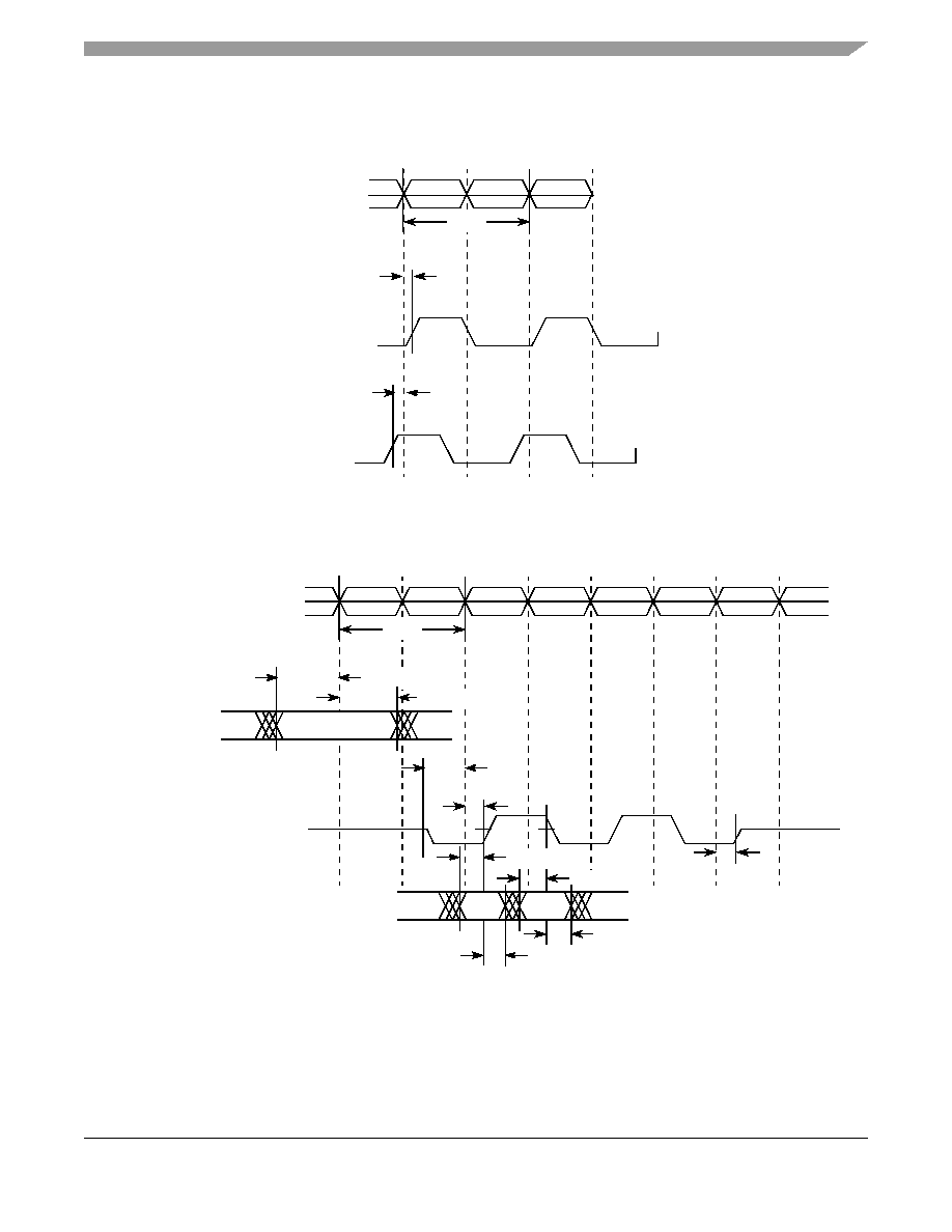
DDR2 and DDR3 SDRAM Controller
Figure 4 shows the DDR2 and DDR3 SDRAM Interface output timing for the MCK to MDQS skew
measurement (tDDKHMH).
Figure 4. Timing Diagram for tDDKHMH
Figure 5 shows the DDR2 and DDR3 SDRAM Interface output timing diagram.
Figure 5. DDR2 and DDR3 SDRAM Interface Output Timing Diagram
MDQS
MCK[n]
tMCK
tDDKHMHmax) = 0.6 ns or 0.375 ns
tDDKHMH(min) = –0.6 ns or -0.375 ns
MDQS
ADDR/CMD
tDDKHAS ,tDDKHCS
tDDKHMH
tDDKLDS
tDDKHDS
MDQ[x]
MDQS[n]
MCK[n]
tMCK
tDDKLDX
tDDKHDX
D1
D0
tDDKHAX ,tDDKHCX
Write A0
NOOP
tDDKHME
tDDKHMP
相關(guān)PDF資料 |
PDF描述 |
|---|---|
| 396-020-521-202 | CARD EDGE 20POS DL .125X.250 BLK |
| MPC8572ECPXARLB | MPU POWERQUICC III 1023-PBGA |
| 395-012-541-204 | CARD EDGE 12POS DL .100X.200 BLK |
| 395-012-541-202 | CARD EDGE 12POS DL .100X.200 BLK |
| HFW13R-2STE1LF | HFW13R-2STE1LF FFC/FPC CONN |
相關(guān)代理商/技術(shù)參數(shù) |
參數(shù)描述 |
|---|---|
| MPC8572ECPXAULD | 功能描述:微處理器 - MPU 1333 EXT TEMP RoHS:否 制造商:Atmel 處理器系列:SAMA5D31 核心:ARM Cortex A5 數(shù)據(jù)總線寬度:32 bit 最大時(shí)鐘頻率:536 MHz 程序存儲(chǔ)器大小:32 KB 數(shù)據(jù) RAM 大小:128 KB 接口類型:CAN, Ethernet, LIN, SPI,TWI, UART, USB 工作電源電壓:1.8 V to 3.3 V 最大工作溫度:+ 85 C 安裝風(fēng)格:SMD/SMT 封裝 / 箱體:FBGA-324 |
| MPC8572ECPXAULE | 功能描述:微處理器 - MPU R211 Enc SnPb 1333 Ext RoHS:否 制造商:Atmel 處理器系列:SAMA5D31 核心:ARM Cortex A5 數(shù)據(jù)總線寬度:32 bit 最大時(shí)鐘頻率:536 MHz 程序存儲(chǔ)器大小:32 KB 數(shù)據(jù) RAM 大小:128 KB 接口類型:CAN, Ethernet, LIN, SPI,TWI, UART, USB 工作電源電壓:1.8 V to 3.3 V 最大工作溫度:+ 85 C 安裝風(fēng)格:SMD/SMT 封裝 / 箱體:FBGA-324 |
| MPC8572ECPXAVND | 功能描述:微處理器 - MPU 1500 EXT TEMP RoHS:否 制造商:Atmel 處理器系列:SAMA5D31 核心:ARM Cortex A5 數(shù)據(jù)總線寬度:32 bit 最大時(shí)鐘頻率:536 MHz 程序存儲(chǔ)器大小:32 KB 數(shù)據(jù) RAM 大小:128 KB 接口類型:CAN, Ethernet, LIN, SPI,TWI, UART, USB 工作電源電壓:1.8 V to 3.3 V 最大工作溫度:+ 85 C 安裝風(fēng)格:SMD/SMT 封裝 / 箱體:FBGA-324 |
| MPC8572ECPXAVNE | 功能描述:微處理器 - MPU R211 Enc SnPb 1500 Ext RoHS:否 制造商:Atmel 處理器系列:SAMA5D31 核心:ARM Cortex A5 數(shù)據(jù)總線寬度:32 bit 最大時(shí)鐘頻率:536 MHz 程序存儲(chǔ)器大小:32 KB 數(shù)據(jù) RAM 大小:128 KB 接口類型:CAN, Ethernet, LIN, SPI,TWI, UART, USB 工作電源電壓:1.8 V to 3.3 V 最大工作溫度:+ 85 C 安裝風(fēng)格:SMD/SMT 封裝 / 箱體:FBGA-324 |
| MPC8572ECVTARLB | 功能描述:微處理器 - MPU RV1.1.1 1067 EXT T RoHS:否 制造商:Atmel 處理器系列:SAMA5D31 核心:ARM Cortex A5 數(shù)據(jù)總線寬度:32 bit 最大時(shí)鐘頻率:536 MHz 程序存儲(chǔ)器大小:32 KB 數(shù)據(jù) RAM 大小:128 KB 接口類型:CAN, Ethernet, LIN, SPI,TWI, UART, USB 工作電源電壓:1.8 V to 3.3 V 最大工作溫度:+ 85 C 安裝風(fēng)格:SMD/SMT 封裝 / 箱體:FBGA-324 |
發(fā)布緊急采購,3分鐘左右您將得到回復(fù)。