- 您現(xiàn)在的位置:買賣IC網(wǎng) > PDF目錄4036 > MPC8548EPXAVHB (Freescale Semiconductor)MPU POWERQUICC III 783-PBGA PDF資料下載
參數(shù)資料
| 型號(hào): | MPC8548EPXAVHB |
| 廠商: | Freescale Semiconductor |
| 文件頁(yè)數(shù): | 38/151頁(yè) |
| 文件大?。?/td> | 0K |
| 描述: | MPU POWERQUICC III 783-PBGA |
| 產(chǎn)品培訓(xùn)模塊: | MPC8548 PowerQUICC III Processors |
| 標(biāo)準(zhǔn)包裝: | 1 |
| 系列: | MPC85xx |
| 處理器類型: | 32-位 MPC85xx PowerQUICC III |
| 速度: | 1.5GHz |
| 電壓: | 1.1V |
| 安裝類型: | 表面貼裝 |
| 封裝/外殼: | 783-BBGA,F(xiàn)CBGA |
| 供應(yīng)商設(shè)備封裝: | 783-FCPBGA(29x29) |
| 包裝: | 托盤 |
第1頁(yè)第2頁(yè)第3頁(yè)第4頁(yè)第5頁(yè)第6頁(yè)第7頁(yè)第8頁(yè)第9頁(yè)第10頁(yè)第11頁(yè)第12頁(yè)第13頁(yè)第14頁(yè)第15頁(yè)第16頁(yè)第17頁(yè)第18頁(yè)第19頁(yè)第20頁(yè)第21頁(yè)第22頁(yè)第23頁(yè)第24頁(yè)第25頁(yè)第26頁(yè)第27頁(yè)第28頁(yè)第29頁(yè)第30頁(yè)第31頁(yè)第32頁(yè)第33頁(yè)第34頁(yè)第35頁(yè)第36頁(yè)第37頁(yè)當(dāng)前第38頁(yè)第39頁(yè)第40頁(yè)第41頁(yè)第42頁(yè)第43頁(yè)第44頁(yè)第45頁(yè)第46頁(yè)第47頁(yè)第48頁(yè)第49頁(yè)第50頁(yè)第51頁(yè)第52頁(yè)第53頁(yè)第54頁(yè)第55頁(yè)第56頁(yè)第57頁(yè)第58頁(yè)第59頁(yè)第60頁(yè)第61頁(yè)第62頁(yè)第63頁(yè)第64頁(yè)第65頁(yè)第66頁(yè)第67頁(yè)第68頁(yè)第69頁(yè)第70頁(yè)第71頁(yè)第72頁(yè)第73頁(yè)第74頁(yè)第75頁(yè)第76頁(yè)第77頁(yè)第78頁(yè)第79頁(yè)第80頁(yè)第81頁(yè)第82頁(yè)第83頁(yè)第84頁(yè)第85頁(yè)第86頁(yè)第87頁(yè)第88頁(yè)第89頁(yè)第90頁(yè)第91頁(yè)第92頁(yè)第93頁(yè)第94頁(yè)第95頁(yè)第96頁(yè)第97頁(yè)第98頁(yè)第99頁(yè)第100頁(yè)第101頁(yè)第102頁(yè)第103頁(yè)第104頁(yè)第105頁(yè)第106頁(yè)第107頁(yè)第108頁(yè)第109頁(yè)第110頁(yè)第111頁(yè)第112頁(yè)第113頁(yè)第114頁(yè)第115頁(yè)第116頁(yè)第117頁(yè)第118頁(yè)第119頁(yè)第120頁(yè)第121頁(yè)第122頁(yè)第123頁(yè)第124頁(yè)第125頁(yè)第126頁(yè)第127頁(yè)第128頁(yè)第129頁(yè)第130頁(yè)第131頁(yè)第132頁(yè)第133頁(yè)第134頁(yè)第135頁(yè)第136頁(yè)第137頁(yè)第138頁(yè)第139頁(yè)第140頁(yè)第141頁(yè)第142頁(yè)第143頁(yè)第144頁(yè)第145頁(yè)第146頁(yè)第147頁(yè)第148頁(yè)第149頁(yè)第150頁(yè)第151頁(yè)
MPC8548E PowerQUICC III Integrated Processor Hardware Specifications, Rev. 9
132
Freescale Semiconductor
Clocking
20.2
CCB/SYSCLK PLL Ratio
The CCB clock is the clock that drives the e500 core complex bus (CCB), and is also called the platform
clock. The frequency of the CCB is set using the following reset signals, as shown in Table 81:
SYSCLK input signal
Binary value on LA[28:31] at power up
Note that there is no default for this PLL ratio; these signals must be pulled to the desired values. Also note
that the DDR data rate is the determining factor in selecting the CCB bus frequency, since the CCB
frequency must equal the DDR data rate.
For specifications on the PCI_CLK, see the PCI 2.2 Specification.
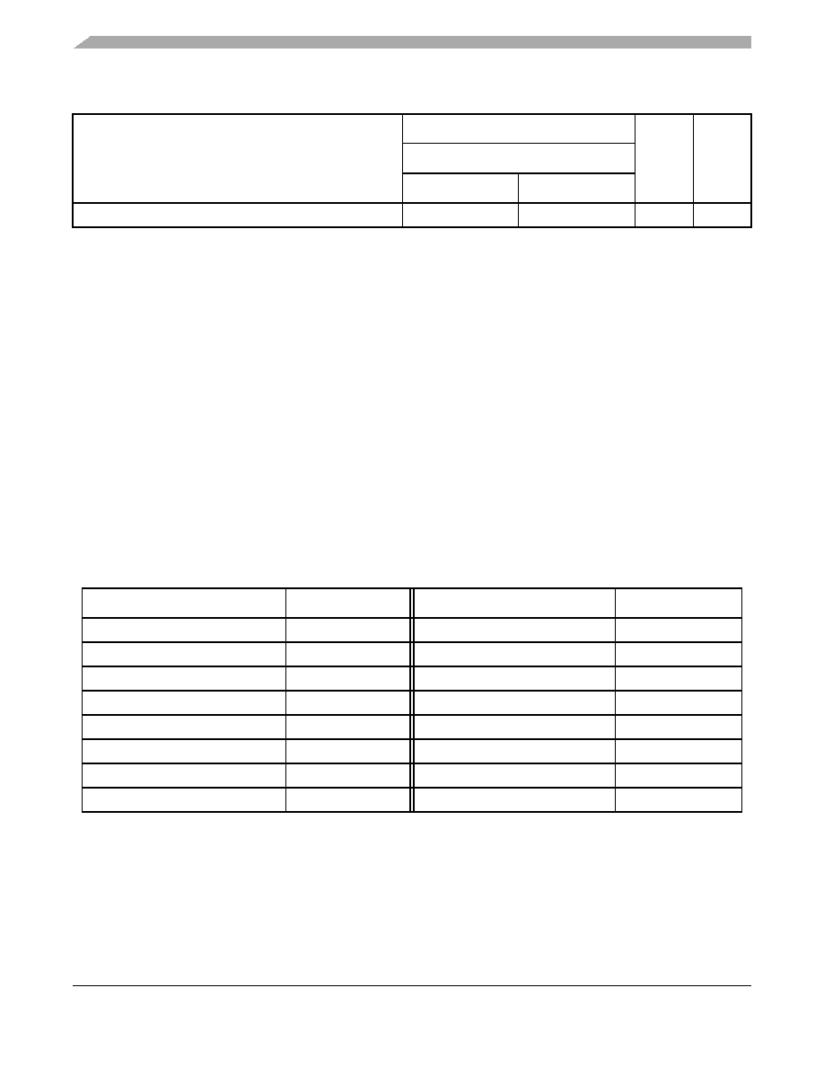
Table 80. Memory Bus Clocking Specifications (MPC8543E)
Characteristic
Maximum Processor Core Frequency
Unit
Notes
800, 1000 MHz
Min
Max
Memory bus clock speed
166
200
MHz
1, 2
Notes:
1. Caution: The CCB clock to SYSCLK ratio and e500 core to CCB clock ratio settings must be chosen such that the resulting
SYSCLK frequency, e500 (core) frequency, and CCB clock frequency do not exceed their respective maximum or minimum
operating frequencies. See Section 20.2, “CCB/SYSCLK PLL Ratio,” and Section 20.3, “e500 Core PLL Ratio,” for ratio
settings.
2. The memory bus speed is half of the DDR/DDR2 data rate, hence, half of the platform clock frequency.
Table 81. CCB Clock Ratio
Binary Value of LA[28:31] Signals
CCB:SYSCLK Ratio
Binary Value of LA[28:31] Signals
CCB:SYSCLK Ratio
0000
16:1
1000
8:1
0001
Reserved
1001
9:1
0010
2:1
1010
10:1
0011
3:1
1011
Reserved
0100
4:1
1100
12:1
0101
5:1
1101
20:1
0110
6:1
1110
Reserved
0111
Reserved
1111
Reserved
相關(guān)PDF資料 |
PDF描述 |
|---|---|
| XC4028XL-2BG352C | IC FPGA C-TEMP 3.3V 2SPD 352MBGA |
| XC4028XL-2BG256I | IC FPGA I-TEMP 3.3V 2SPD 256PBGA |
| FMC40DRYH-S93 | CONN EDGECARD 80POS .100 DIP SLD |
| MPC8548ECVTATGB | MPU POWERQUICC III 783-PBGA |
| MPC8548ECPXATGB | MPU POWERQUICC III 783-PBGA |
相關(guān)代理商/技術(shù)參數(shù) |
參數(shù)描述 |
|---|---|
| MPC8548EPXAVHD | 功能描述:微處理器 - MPU PQ38 PB ST WE 1500 R3.0 RoHS:否 制造商:Atmel 處理器系列:SAMA5D31 核心:ARM Cortex A5 數(shù)據(jù)總線寬度:32 bit 最大時(shí)鐘頻率:536 MHz 程序存儲(chǔ)器大小:32 KB 數(shù)據(jù) RAM 大小:128 KB 接口類型:CAN, Ethernet, LIN, SPI,TWI, UART, USB 工作電源電壓:1.8 V to 3.3 V 最大工作溫度:+ 85 C 安裝風(fēng)格:SMD/SMT 封裝 / 箱體:FBGA-324 |
| MPC8548EVTAQGA | 制造商:Freescale Semiconductor 功能描述:MPC85XX RISC 32-BIT CMOS 1GHZ 1.8V/2.5V/3.3V 783-PIN BGA TRA - Bulk |
| MPC8548EVTAQGB | 功能描述:微處理器 - MPU FG PQ38 8548 PB Free RoHS:否 制造商:Atmel 處理器系列:SAMA5D31 核心:ARM Cortex A5 數(shù)據(jù)總線寬度:32 bit 最大時(shí)鐘頻率:536 MHz 程序存儲(chǔ)器大小:32 KB 數(shù)據(jù) RAM 大小:128 KB 接口類型:CAN, Ethernet, LIN, SPI,TWI, UART, USB 工作電源電壓:1.8 V to 3.3 V 最大工作溫度:+ 85 C 安裝風(fēng)格:SMD/SMT 封裝 / 箱體:FBGA-324 |
| MPC8548EVTAQGD | 功能描述:微處理器 - MPU PQ38 ST WE 1000 R3.0 RoHS:否 制造商:Atmel 處理器系列:SAMA5D31 核心:ARM Cortex A5 數(shù)據(jù)總線寬度:32 bit 最大時(shí)鐘頻率:536 MHz 程序存儲(chǔ)器大小:32 KB 數(shù)據(jù) RAM 大小:128 KB 接口類型:CAN, Ethernet, LIN, SPI,TWI, UART, USB 工作電源電壓:1.8 V to 3.3 V 最大工作溫度:+ 85 C 安裝風(fēng)格:SMD/SMT 封裝 / 箱體:FBGA-324 |
| MPC8548EVTATGB | 功能描述:微處理器 - MPU FG PQ38 8548 PB Free RoHS:否 制造商:Atmel 處理器系列:SAMA5D31 核心:ARM Cortex A5 數(shù)據(jù)總線寬度:32 bit 最大時(shí)鐘頻率:536 MHz 程序存儲(chǔ)器大小:32 KB 數(shù)據(jù) RAM 大小:128 KB 接口類型:CAN, Ethernet, LIN, SPI,TWI, UART, USB 工作電源電壓:1.8 V to 3.3 V 最大工作溫度:+ 85 C 安裝風(fēng)格:SMD/SMT 封裝 / 箱體:FBGA-324 |
發(fā)布緊急采購(gòu),3分鐘左右您將得到回復(fù)。