- 您現(xiàn)在的位置:買賣IC網(wǎng) > PDF目錄45363 > MPC8347ECVRAGF (FREESCALE SEMICONDUCTOR INC) 32-BIT, 400 MHz, RISC PROCESSOR, PBGA620 PDF資料下載
參數(shù)資料
| 型號: | MPC8347ECVRAGF |
| 廠商: | FREESCALE SEMICONDUCTOR INC |
| 元件分類: | 微控制器/微處理器 |
| 英文描述: | 32-BIT, 400 MHz, RISC PROCESSOR, PBGA620 |
| 封裝: | 29 X 29 MM, 2.46 MM HEIGHT, 1 MM PITCH, LEAD FREE, PLASTIC, BGA-620 |
| 文件頁數(shù): | 99/102頁 |
| 文件大小: | 1094K |
| 代理商: | MPC8347ECVRAGF |
第1頁第2頁第3頁第4頁第5頁第6頁第7頁第8頁第9頁第10頁第11頁第12頁第13頁第14頁第15頁第16頁第17頁第18頁第19頁第20頁第21頁第22頁第23頁第24頁第25頁第26頁第27頁第28頁第29頁第30頁第31頁第32頁第33頁第34頁第35頁第36頁第37頁第38頁第39頁第40頁第41頁第42頁第43頁第44頁第45頁第46頁第47頁第48頁第49頁第50頁第51頁第52頁第53頁第54頁第55頁第56頁第57頁第58頁第59頁第60頁第61頁第62頁第63頁第64頁第65頁第66頁第67頁第68頁第69頁第70頁第71頁第72頁第73頁第74頁第75頁第76頁第77頁第78頁第79頁第80頁第81頁第82頁第83頁第84頁第85頁第86頁第87頁第88頁第89頁第90頁第91頁第92頁第93頁第94頁第95頁第96頁第97頁第98頁當(dāng)前第99頁第100頁第101頁第102頁
MPC8347E PowerQUICC II Pro Integrated Host Processor Hardware Specifications, Rev. 11
96
Freescale Semiconductor
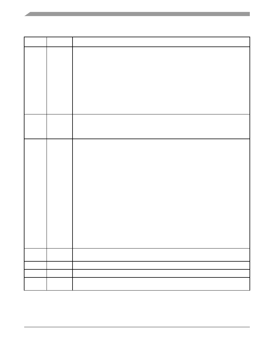
Document Revision History
8
2/2007
Page 1, updated first paragraph to reflect PowerQUICC II information. Updated note after second
paragraph.
In the features list in Section 1, “Overview,” corrected DDR data rate to show:
266 MHz for PBGA parts for all silicon revisions
333 MHz for DDR for TBGA parts for silicon Rev. 1.x
table footnote to designate rates that apply only to the TBGA package.
In Figure 43, “JTAG Interface Connection,” updated with new figure.
In Section 23, “Ordering Information,” replicated note from document introduction.
In Section 23.1, “Part Numbers Fully Addressed by This Document,” replaced third sentence of first
paragraph directing customer to product summary page for available frequency configuration parts.
Updated back page information.
7
8/2006
Changed all references to revision 2.0 silicon to revision 3.0 silicon.
Changed VIH minimum value in Table 36, “JTAG Interface DC Electrical Characteristics,” to
OVDD –0.3.
In Table 60, “Suggested PLL Configurations,” deleted reference-number rows 902 and 703.
6
3/2006
Section 2, “Electrical Characteristics,” moved to second section and all other section, table, and
figure numbering change accordingly.
Table 7, “CLKIN AC Timing Specifications:” Changed max rise and fall time from 1.2 to 2.3.
Table 22, “GMII Receive AC Timing Specifications:” Changed min tTTKHDX from 0.5 to 1.0.
Table 30, “MII Management AC Timing Specifications:” Changed max value of tMDKHDX from 70 to
170.
Table 34, “Local Bus General Timing Parameters—DLL on:” Changed min tLBIVKH2 from 1.7 to 2.2.
Table 36, “JTAG interface DC Electrical Characteristics:” Changed VIH input high voltage min to 2.0.
Table 54, “Operating Frequencies for TBGA:”
Updated TBD values.
Changed maximum coherent system bus frequency for TBGA 667-MHz device to 333 MHz.
Table 55, “Operating Frequencies for PBGA:”
Updated TBD values.
Changed PBGA maximum coherent system bus frequency to 266 MHz, and maximum DDR
memory bus frequency to 133 MHz.
Table 60, “Suggested PLL Configurations”: Removed some values from suggested PLL
configurations for reference numbers 902, 922, 903, and 923.
Table 67, “Part Numbering Nomenclature”: Updated TBD values in note 1.
Added Table 68, “SVR Settings.”
Added Section 23.2, “Part Marking.”
5
10/2005
In Table 57, updated AAVID 30x30x9.4 mm Pin Fin (natural convection) junction-to-ambient thermal
resistance, from 11 to 10.
4
9/2005
Added Table 2, “MPC8347E Typical I/O Power Dissipation.”
3
8/2005
Table 1: Updated values for power dissipation that were TBD in Revision 2.
2
5/2005
Table 1: Typical values for power dissipation are changed to TBD.
Table 48: Footnote numbering was wrong. THERM0 should have footnote 9 instead of 8.
Table 66. Document Revision History (continued)
Revision
Date
Substantive Change(s)
相關(guān)PDF資料 |
PDF描述 |
|---|---|
| MPC8347ECVRAJD | 32-BIT, 533 MHz, RISC PROCESSOR, PBGA620 |
| MPC8347ECZQADD | 32-BIT, 266 MHz, RISC PROCESSOR, PBGA620 |
| MPC8347CVVALF | 32-BIT, 667 MHz, RISC PROCESSOR, PBGA672 |
| MPC8347CZUADF | 32-BIT, 266 MHz, RISC PROCESSOR, PBGA672 |
| MPC8347ZQADF | 32-BIT, 266 MHz, RISC PROCESSOR, PBGA620 |
相關(guān)代理商/技術(shù)參數(shù) |
參數(shù)描述 |
|---|---|
| MPC8347ECVRAGFB | 制造商:FREESCALE 制造商全稱:Freescale Semiconductor, Inc 功能描述:MPC8347EA PowerQUICC II Pro Integrated Host Processor Hardware Specifications |
| MPC8347ECVRAJDB | 制造商:FREESCALE 制造商全稱:Freescale Semiconductor, Inc 功能描述:MPC8347EA PowerQUICC II Pro Integrated Host Processor Hardware Specifications |
| MPC8347ECVRAJFB | 制造商:FREESCALE 制造商全稱:Freescale Semiconductor, Inc 功能描述:MPC8347EA PowerQUICC II Pro Integrated Host Processor Hardware Specifications |
| MPC8347ECVRALDB | 制造商:FREESCALE 制造商全稱:Freescale Semiconductor, Inc 功能描述:MPC8347EA PowerQUICC II Pro Integrated Host Processor Hardware Specifications |
| MPC8347ECVRALFB | 制造商:FREESCALE 制造商全稱:Freescale Semiconductor, Inc 功能描述:MPC8347EA PowerQUICC II Pro Integrated Host Processor Hardware Specifications |
發(fā)布緊急采購,3分鐘左右您將得到回復(fù)。