- 您現(xiàn)在的位置:買賣IC網(wǎng) > PDF目錄3947 > MPC8313VRAFFB (Freescale Semiconductor)IC MPU POWERQUICC II PRO 516PBGA PDF資料下載
參數(shù)資料
| 型號: | MPC8313VRAFFB |
| 廠商: | Freescale Semiconductor |
| 文件頁數(shù): | 41/99頁 |
| 文件大小: | 0K |
| 描述: | IC MPU POWERQUICC II PRO 516PBGA |
| 標(biāo)準(zhǔn)包裝: | 40 |
| 系列: | MPC83xx |
| 處理器類型: | 32-位 MPC83xx PowerQUICC II Pro |
| 速度: | 333MHz |
| 電壓: | 0.95 V ~ 1.05 V |
| 安裝類型: | 表面貼裝 |
| 封裝/外殼: | 516-BBGA 裸露焊盤 |
| 供應(yīng)商設(shè)備封裝: | 516-PBGAPGE(27x27) |
| 包裝: | 托盤 |
| 配用: | MPC8313E-RDB-ND - BOARD PROCESSOR |
第1頁第2頁第3頁第4頁第5頁第6頁第7頁第8頁第9頁第10頁第11頁第12頁第13頁第14頁第15頁第16頁第17頁第18頁第19頁第20頁第21頁第22頁第23頁第24頁第25頁第26頁第27頁第28頁第29頁第30頁第31頁第32頁第33頁第34頁第35頁第36頁第37頁第38頁第39頁第40頁當(dāng)前第41頁第42頁第43頁第44頁第45頁第46頁第47頁第48頁第49頁第50頁第51頁第52頁第53頁第54頁第55頁第56頁第57頁第58頁第59頁第60頁第61頁第62頁第63頁第64頁第65頁第66頁第67頁第68頁第69頁第70頁第71頁第72頁第73頁第74頁第75頁第76頁第77頁第78頁第79頁第80頁第81頁第82頁第83頁第84頁第85頁第86頁第87頁第88頁第89頁第90頁第91頁第92頁第93頁第94頁第95頁第96頁第97頁第98頁第99頁
MPC8313E PowerQUICC II Pro Processor Hardware Specifications, Rev. 4
46
Freescale Semiconductor
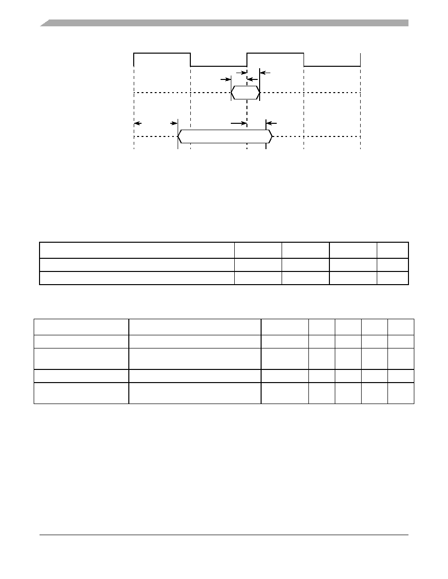
Figure 35. USB Signals
10.2
On-Chip USB PHY
This section describes the DC and AC electrical specifications for the on-chip USB PHY of the
MPC8313E. See Chapter 7 in the USB Specifications Rev. 2, for more information.
This table provides the USB clock input (USB_CLK_IN) DC timing specifications.
This table provides the USB clock input (USB_CLK_IN) AC timing specifications.
Table 42. USB_CLK_IN DC Electrical Characteristics
Parameter
Symbol
Min
Max
Unit
Input high voltage
VIH
2.7
NVDD +0.3
V
Input low voltage
VIL
–0.3
0.4
V
Table 43. USB_CLK_IN AC Timing Specifications
Parameter/Condition
Conditions
Symbol
Min
Typ
Max
Unit
Frequency range
—
fUSB_CLK_IN
—24
48
MHz
Clock frequency tolerance
—
tCLK_TOL
–0.005
0
0.005
%
Reference clock duty cycle
Measured at 1.6 V
tCLK_DUTY
40
50
60
%
Total input jitter/time interval
error
Peak-to-peak value measured with a second
order high-pass filter of 500 kHz bandwidth
tCLK_PJ
——
200
ps
Output Signals
tUSKHOV
USBDR_CLK
Input Signals
tUSIXKH
tUSIVKH
tUSKHOX
相關(guān)PDF資料 |
PDF描述 |
|---|---|
| MPC8313ECZQAFFB | IC MPU POWERQUICC II PRO 516PBGA |
| MPC8313ECVRAFFB | IC MPU POWERQUICC II PRO 516PBGA |
| MPC8313CVRAFFB | IC MPU POWERQUICC II PRO 516PBGA |
| 355-012-521-201 | CARDEDGE 12POS DL .156 LOPRO BLK |
| MPC8378EVRANG | MPU PWRQUICC II 800MHZ 689TEPBGA |
相關(guān)代理商/技術(shù)參數(shù) |
參數(shù)描述 |
|---|---|
| MPC8313VRAFFC | 功能描述:微處理器 - MPU 8313 REV2.2 NO ENC RoHS:否 制造商:Atmel 處理器系列:SAMA5D31 核心:ARM Cortex A5 數(shù)據(jù)總線寬度:32 bit 最大時鐘頻率:536 MHz 程序存儲器大小:32 KB 數(shù)據(jù) RAM 大小:128 KB 接口類型:CAN, Ethernet, LIN, SPI,TWI, UART, USB 工作電源電壓:1.8 V to 3.3 V 最大工作溫度:+ 85 C 安裝風(fēng)格:SMD/SMT 封裝 / 箱體:FBGA-324 |
| MPC8313VRAGDB | 功能描述:微處理器 - MPU PBGA W/O ENCR RoHS:否 制造商:Atmel 處理器系列:SAMA5D31 核心:ARM Cortex A5 數(shù)據(jù)總線寬度:32 bit 最大時鐘頻率:536 MHz 程序存儲器大小:32 KB 數(shù)據(jù) RAM 大小:128 KB 接口類型:CAN, Ethernet, LIN, SPI,TWI, UART, USB 工作電源電壓:1.8 V to 3.3 V 最大工作溫度:+ 85 C 安裝風(fēng)格:SMD/SMT 封裝 / 箱體:FBGA-324 |
| MPC8313VRAGDC | 功能描述:微處理器 - MPU 8313 REV2.2 NO ENC RoHS:否 制造商:Atmel 處理器系列:SAMA5D31 核心:ARM Cortex A5 數(shù)據(jù)總線寬度:32 bit 最大時鐘頻率:536 MHz 程序存儲器大小:32 KB 數(shù)據(jù) RAM 大小:128 KB 接口類型:CAN, Ethernet, LIN, SPI,TWI, UART, USB 工作電源電壓:1.8 V to 3.3 V 最大工作溫度:+ 85 C 安裝風(fēng)格:SMD/SMT 封裝 / 箱體:FBGA-324 |
| MPC8313VRGDD | 制造商:FREESCALE 制造商全稱:Freescale Semiconductor, Inc 功能描述:PowerQUICC? II Pro Processor Hardware Specifications |
| MPC8313VRGDDA | 制造商:FREESCALE 制造商全稱:Freescale Semiconductor, Inc 功能描述:PowerQUICC? II Pro Processor Hardware Specifications |
發(fā)布緊急采購,3分鐘左右您將得到回復(fù)。