- 您現(xiàn)在的位置:買賣IC網(wǎng) > PDF目錄4048 > MPC8265AZUMHBC (Freescale Semiconductor)IC MPU POWERQUICC II 480-TBGA PDF資料下載
參數(shù)資料
| 型號: | MPC8265AZUMHBC |
| 廠商: | Freescale Semiconductor |
| 文件頁數(shù): | 15/50頁 |
| 文件大小: | 0K |
| 描述: | IC MPU POWERQUICC II 480-TBGA |
| 標(biāo)準包裝: | 21 |
| 系列: | MPC82xx |
| 處理器類型: | 32-位 MPC82xx PowerQUICC II |
| 速度: | 266MHz |
| 電壓: | 2V |
| 安裝類型: | 表面貼裝 |
| 封裝/外殼: | 480-LBGA |
| 供應(yīng)商設(shè)備封裝: | 408-TBGA(37.5x37.5) |
| 包裝: | 托盤 |
第1頁第2頁第3頁第4頁第5頁第6頁第7頁第8頁第9頁第10頁第11頁第12頁第13頁第14頁當(dāng)前第15頁第16頁第17頁第18頁第19頁第20頁第21頁第22頁第23頁第24頁第25頁第26頁第27頁第28頁第29頁第30頁第31頁第32頁第33頁第34頁第35頁第36頁第37頁第38頁第39頁第40頁第41頁第42頁第43頁第44頁第45頁第46頁第47頁第48頁第49頁第50頁
MPC8260A PowerQUICC II Integrated Communications Processor Hardware Specifications, Rev. 2.0
22
Freescale Semiconductor
Electrical and Thermal Characteristics
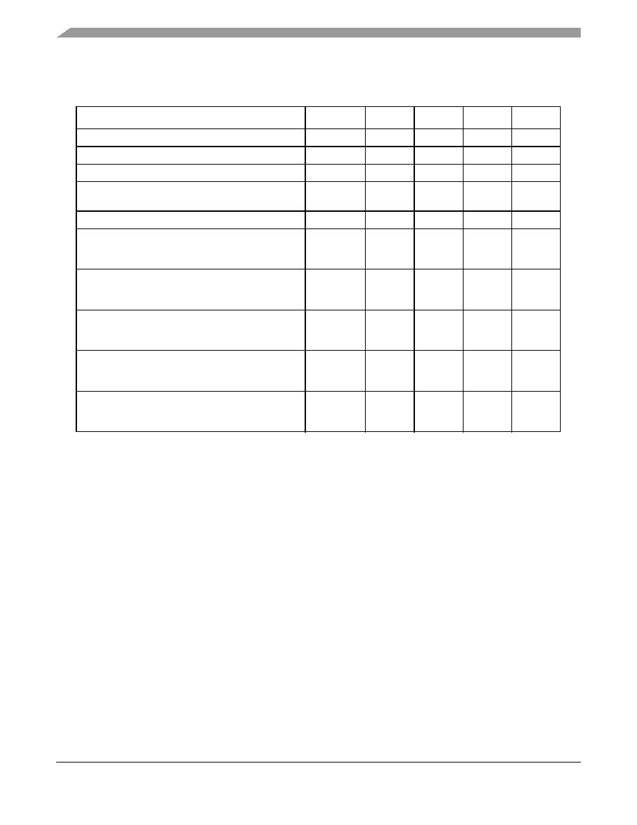
Table 12 lists the JTAG timings.
NOTE
The UPM machine outputs change on the internal tick determined by the
memory controller programming; the AC specifications are relative to the
internal tick. Note that SDRAM and GPCM machine outputs change on
CLKin’s rising edge.
Table 12. JTAG Timings1
Parameter
Symbol2
Min
Max
Unit
Notes
JTAG external clock frequency of operation
fJTG
025
MHz
—
JTAG external clock cycle time
tJTG
40
—
ns
—
JTAG external clock pulse width measured at 1.4V
tJTKHKL
20
—
ns
—
JTAG external clock rise and fall times
tJTGR and
tJTGF
05
ns
6
TRST assert time
tTRST
25
—
ns
3, 6
Input setup times
Boundary-scan data
TMS, TDI
tJTDVKH
tJTIVKH
4
—
ns
4, 7
Input hold times
Boundary-scan data
TMS, TDI
tJTDXKH
tJTIXKH
10
—
ns
4, 7
Output valid times
Boundary-scan data
TDO
tJTKLDV
tJTKLOV
—
25
ns
5, 7
5. 7
Output hold times
Boundary-scan data
TDO
tJTKLDX
tJTKLOX
1
—
ns
5, 7
JTAG external clock to output high impedance
Boundary-scan data
TDO
tJTKLDZ
tJTKLOZ
1
25
ns
5, 6
1 All outputs are measured from the midpoint voltage of the falling/rising edge of t
TCLK to the midpoint of the signal
in question. The output timings are measured at the pins. All output timings assume a purely resistive 50-
Ω load.
Time-of-flight delays must be added for trace lengths, vias, and connectors in the system.
2 The symbols used for timing specifications herein follow the pattern of t
(first two letters of functional block)(signal)(state)
(reference)(state) for inputs and t((first two letters of functional block)(reference)(state)(signal)(state) for outputs. For example,
tJTDVKH symbolizes JTAG device timing (JT) with respect to the time data input signals (D) reaching the valid state
(V) relative to the tJTG clock reference (K) going to the high (H) state or setup time. Also, tJTDXKH symbolizes JTAG
timing (JT) with respect to the time data input signals (D) went invalid (X) relative to the tJTG clock reference (K)
going to the high (H) state. Note that, in general, the clock reference symbol representation is based on three letters
representing the clock of a particular functional. For rise and fall times, the latter convention is used with the
appropriate letter: R (rise) or F (fall).
3 TRST is an asynchronous level sensitive signal. The setup time is for test purposes only.
4 Non-JTAG signal input timing with respect to t
TCLK.
5 Non-JTAG signal output timing with respect to t
TCLK.
6 Guaranteed by design.
7 Guaranteed by design and device characterization.
相關(guān)PDF資料 |
PDF描述 |
|---|---|
| XC4052XL-1HQ240I | IC FPGA I-TEMP 3.3V 1SPD 240HQFP |
| XC4036XL-3BG352C | IC FPGA C-TEMP 3.3V 3SPD 352MBGA |
| AMC65DRTS-S93 | CONN EDGECARD 130PS DIP .100 SLD |
| MPC603RRX266TC | IC MPU 32BIT 266MHZ 255-CBGA |
| MPC8536AVTAQGA | MPU POWERQUICC III 783FCPBGA |
相關(guān)代理商/技術(shù)參數(shù) |
參數(shù)描述 |
|---|---|
| MPC8265AZUPIBC | 功能描述:微處理器 - MPU POWER QUICC II HIP4C RoHS:否 制造商:Atmel 處理器系列:SAMA5D31 核心:ARM Cortex A5 數(shù)據(jù)總線寬度:32 bit 最大時鐘頻率:536 MHz 程序存儲器大小:32 KB 數(shù)據(jù) RAM 大小:128 KB 接口類型:CAN, Ethernet, LIN, SPI,TWI, UART, USB 工作電源電壓:1.8 V to 3.3 V 最大工作溫度:+ 85 C 安裝風(fēng)格:SMD/SMT 封裝 / 箱體:FBGA-324 |
| MPC8265AZUPJDB | 制造商:Motorola Inc 功能描述:Ic, Microprocessor, 32-bit, Cmos, Bga, 480pin, Plastic |
| MPC8265AZUPJDC | 功能描述:微處理器 - MPU POWER QUICC II HIP4C RoHS:否 制造商:Atmel 處理器系列:SAMA5D31 核心:ARM Cortex A5 數(shù)據(jù)總線寬度:32 bit 最大時鐘頻率:536 MHz 程序存儲器大小:32 KB 數(shù)據(jù) RAM 大小:128 KB 接口類型:CAN, Ethernet, LIN, SPI,TWI, UART, USB 工作電源電壓:1.8 V to 3.3 V 最大工作溫度:+ 85 C 安裝風(fēng)格:SMD/SMT 封裝 / 箱體:FBGA-324 |
| MPC8265CVR | 制造商:MOTOROLA 制造商全稱:Motorola, Inc 功能描述:MPC826xA (HiP4) Family Hardware Specifications |
| MPC8265CZU | 制造商:MOTOROLA 制造商全稱:Motorola, Inc 功能描述:MPC826xA (HiP4) Family Hardware Specifications |
發(fā)布緊急采購,3分鐘左右您將得到回復(fù)。