- 您現(xiàn)在的位置:買賣IC網(wǎng) > PDF目錄4094 > MPC8245ARVV400D (Freescale Semiconductor)IC MPU 32BIT 400MHZ 352-TBGA PDF資料下載
參數(shù)資料
第1頁(yè)第2頁(yè)第3頁(yè)第4頁(yè)第5頁(yè)第6頁(yè)第7頁(yè)第8頁(yè)第9頁(yè)第10頁(yè)第11頁(yè)第12頁(yè)第13頁(yè)第14頁(yè)當(dāng)前第15頁(yè)第16頁(yè)第17頁(yè)第18頁(yè)第19頁(yè)第20頁(yè)第21頁(yè)第22頁(yè)第23頁(yè)第24頁(yè)第25頁(yè)第26頁(yè)第27頁(yè)第28頁(yè)第29頁(yè)第30頁(yè)第31頁(yè)第32頁(yè)第33頁(yè)第34頁(yè)第35頁(yè)第36頁(yè)第37頁(yè)第38頁(yè)第39頁(yè)第40頁(yè)第41頁(yè)第42頁(yè)第43頁(yè)第44頁(yè)第45頁(yè)第46頁(yè)第47頁(yè)第48頁(yè)第49頁(yè)第50頁(yè)第51頁(yè)第52頁(yè)第53頁(yè)第54頁(yè)第55頁(yè)第56頁(yè)第57頁(yè)第58頁(yè)第59頁(yè)第60頁(yè)第61頁(yè)第62頁(yè)第63頁(yè)第64頁(yè)第65頁(yè)第66頁(yè)第67頁(yè)第68頁(yè)
MPC8245 Integrated Processor Hardware Specifications, Rev. 10
22
Freescale Semiconductor
Electrical and Thermal Characteristics
PCI_SYNC_IN, respectively.
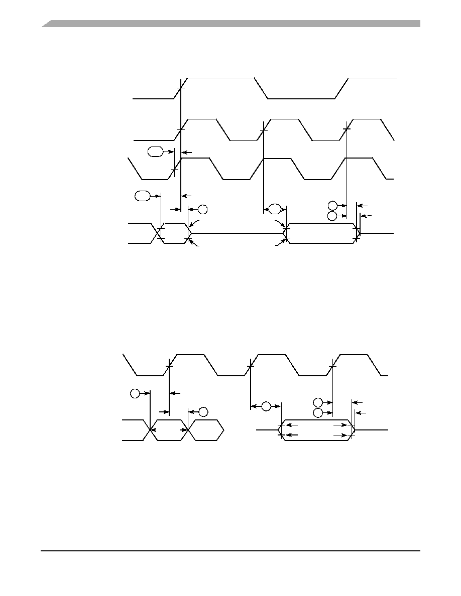
Figure 11. Input/Output Timing Diagram Referenced to SDRAM_SYNC_IN
Figure 12. Input/Output Timing Diagram Referenced to PCI_SYNC_IN
11a
VM = Midpoint voltage (1.4 V).
Memory
10b-d
Inputs/Outputs
13b
14b
VM
SDRAM_SYNC_IN
Input Timing
Output Timing
12b-d
2.0 V
0.8 V
2.0 V
Tos
11a = Input hold time of SDRAM_SYNC_IN to memory.
12b-d = sys_logic_clk to output valid timing.
13b = Output hold time for non-PCI signals.
14b = SDRAM-SYNC_IN to output high-impedance timing for non-PCI signals.
Tos = Offset timing required to align sys_logic_clk with SDRAM_SYNC_IN. The SDRAM_SYNC_IN signal
sys_logic_clk
VM
PCI_SYNC_IN
VM
is adjusted by the DLL to accommodate for internal delay. This causes SDRAM_SYNC_IN to appear
before sys_logic_clk once the DLL locks.
(after DLL locks)
Shown in 2:1 Mode
Notes:
10b-d = Input signals valid timing.
OVDD ÷ 2
10a
11c
PCI_SYNC_IN
PCI
12a
13a
14a
OVDD ÷ 2
0.4
× OV
DD
0.615
× OVDD
0.285
× OVDD
Input Timing
Output Timing
Inputs/Outputs
相關(guān)PDF資料 |
PDF描述 |
|---|---|
| MPC8245ARZU400D | IC MPU 32BIT 400MHZ 352-TBGA |
| MPC860TCVR50D4 | IC MPU POWERQUICC 50MHZ 357PBGA |
| XC3S1500L-4FGG456C | SPARTAN-3A FPGA 1.5M STD 456FBGA |
| MPC860TCZQ50D4 | IC MPU POWERQUICC 50MHZ 357PBGA |
| FMC31DRYH-S734 | CONN EDGECARD 62POS DIP .100 SLD |
相關(guān)代理商/技術(shù)參數(shù) |
參數(shù)描述 |
|---|---|
| MPC8245ARZU400D | 功能描述:微處理器 - MPU INTEGRATED HOST PROC RoHS:否 制造商:Atmel 處理器系列:SAMA5D31 核心:ARM Cortex A5 數(shù)據(jù)總線寬度:32 bit 最大時(shí)鐘頻率:536 MHz 程序存儲(chǔ)器大小:32 KB 數(shù)據(jù) RAM 大小:128 KB 接口類型:CAN, Ethernet, LIN, SPI,TWI, UART, USB 工作電源電壓:1.8 V to 3.3 V 最大工作溫度:+ 85 C 安裝風(fēng)格:SMD/SMT 封裝 / 箱體:FBGA-324 |
| MPC8245ARZU400D | 制造商:Freescale Semiconductor 功能描述:IC 32BIT MPU 400MHZ BGA-352 |
| MPC8245ARZU466D | 制造商:FREESCALE 制造商全稱:Freescale Semiconductor, Inc 功能描述:Part Number Specification for the MPC8245ARZUnnnX Series |
| MPC8245EC | 制造商:FREESCALE 制造商全稱:Freescale Semiconductor, Inc 功能描述:MPC8245 Integrated Processor Hardware Specifications |
| MPC8245ECS02AD | 制造商:FREESCALE 制造商全稱:Freescale Semiconductor, Inc 功能描述:MPC8245 Integrated Processor Hardware Specifications |
發(fā)布緊急采購(gòu),3分鐘左右您將得到回復(fù)。