- 您現(xiàn)在的位置:買賣IC網(wǎng) > PDF目錄45339 > MPC5603CF1VLL4 (FREESCALE SEMICONDUCTOR INC) MICROCONTROLLER, PQFP100 PDF資料下載
參數(shù)資料
| 型號: | MPC5603CF1VLL4 |
| 廠商: | FREESCALE SEMICONDUCTOR INC |
| 元件分類: | 微控制器/微處理器 |
| 英文描述: | MICROCONTROLLER, PQFP100 |
| 封裝: | 14 X 14 MM, 1.40 MM HEIGHT, 0.50 MM PITCH, LQFP-100 |
| 文件頁數(shù): | 37/106頁 |
| 文件大小: | 1693K |
| 代理商: | MPC5603CF1VLL4 |
第1頁第2頁第3頁第4頁第5頁第6頁第7頁第8頁第9頁第10頁第11頁第12頁第13頁第14頁第15頁第16頁第17頁第18頁第19頁第20頁第21頁第22頁第23頁第24頁第25頁第26頁第27頁第28頁第29頁第30頁第31頁第32頁第33頁第34頁第35頁第36頁當前第37頁第38頁第39頁第40頁第41頁第42頁第43頁第44頁第45頁第46頁第47頁第48頁第49頁第50頁第51頁第52頁第53頁第54頁第55頁第56頁第57頁第58頁第59頁第60頁第61頁第62頁第63頁第64頁第65頁第66頁第67頁第68頁第69頁第70頁第71頁第72頁第73頁第74頁第75頁第76頁第77頁第78頁第79頁第80頁第81頁第82頁第83頁第84頁第85頁第86頁第87頁第88頁第89頁第90頁第91頁第92頁第93頁第94頁第95頁第96頁第97頁第98頁第99頁第100頁第101頁第102頁第103頁第104頁第105頁第106頁
MPC5604B/C Microcontroller Data Sheet, Rev. 8
Electrical characteristics
Freescale Semiconductor
36
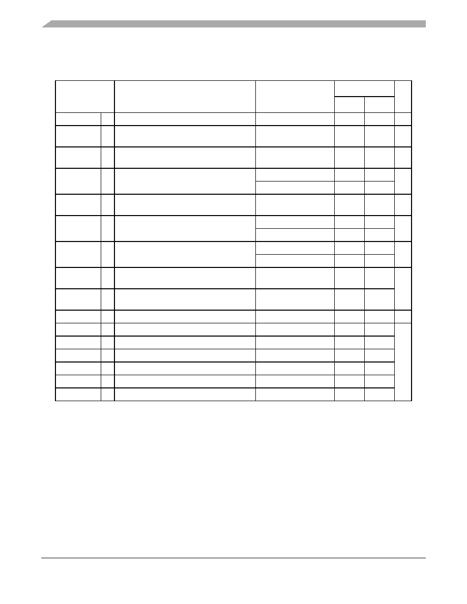
4.5
Recommended operating conditions
Table 8. Recommended operating conditions (3.3 V)
Symbol
Parameter
Conditions
Value
Unit
Min
Max
VSS
SR Digital ground on VSS_HV pins
—
0
V
VDD
1
1 100 nF capacitance needs to be provided between each V
DD/VSS pair
SR Voltage on VDD_HV pins with respect to
ground (VSS)
—3.0
3.6
V
VSS_LV
2
2 330 nF capacitance needs to be provided between each V
DD_LV/VSS_LV supply pair.
SR Voltage on VSS_LV (low voltage digital
supply) pins with respect to ground (VSS)
—VSS0.1 VSS+0.1
V
VDD_BV
3
3 400 nF capacitance needs to be provided between V
DD_BV and the nearest VSS_LV (higher value may be needed
depending on external regulator characteristics).
SR Voltage on VDD_BV pin (regulator supply)
with respect to ground (VSS)
—3.0
3.6
V
Relative to VDD
VDD0.1 VDD+0.1
VSS_ADC
SR Voltage on VSS_HV_ADC (ADC reference)
pin with respect to ground (VSS)
—VSS0.1 VSS+0.1
V
VDD_ADC
4
4 100 nF capacitance needs to be provided between V
DD_ADC/VSS_ADC pair.
SR Voltage on VDD_HV_ADC pin (ADC
reference) with respect to ground (VSS)
—3.05
5 Full electrical specification cannot be guaranteed when voltage drops below 3.0 V. In particular, ADC electrical
characteristics and I/Os DC electrical specification may not be guaranteed. When voltage drops below VLVDHVL,
device is reset.
3.6
V
Relative to VDD
VDD0.1 VDD+0.1
VIN
SR Voltage on any GPIO pin with respect to
ground (VSS)
—VSS0.1
—
V
Relative to VDD
—VDD+0.1
IINJPAD
SR Injected input current on any pin during
overload condition
—
55
mA
IINJSUM
SR Absolute sum of all injected input currents
during overload condition
—
50
TVDD
SR VDD slope to ensure correct power up
6
6 Guaranteed by device validation
—
0.25
V/s
TA C-Grade Part SR Ambient temperature under bias
fCPU < 64 MHz
40
85
°C
TJ C-Grade Part SR Junction temperature under bias
—
40
110
TA V-Grade Part SR Ambient temperature under bias
fCPU < 64 MHz
40
105
TJ V-Grade Part SR Junction temperature under bias
—
40
130
TA M-Grade Part SR Ambient temperature under bias
fCPU < 64 MHz
40
125
TJ M-Grade Part SR Junction temperature under bias
—
40
150
相關(guān)PDF資料 |
PDF描述 |
|---|---|
| MPC5602BF1MLH4R | MICROCONTROLLER, PQFP64 |
| MPC5602BF1VLH6 | MICROCONTROLLER, PQFP64 |
| MPC5602BF1VLQ4 | MICROCONTROLLER, PQFP144 |
| MPC5603CF1MLH6 | MICROCONTROLLER, PQFP64 |
| MPC5602BF1MLL6R | MICROCONTROLLER, PQFP100 |
相關(guān)代理商/技術(shù)參數(shù) |
參數(shù)描述 |
|---|---|
| MPC5603PEF0MLL7R | 制造商:FREESCALE 制造商全稱:Freescale Semiconductor, Inc 功能描述:microcontroller units (MCUs) |
| MPC5603PEF0MLQ7R | 制造商:FREESCALE 制造商全稱:Freescale Semiconductor, Inc 功能描述:microcontroller units (MCUs) |
| MPC5603PEF0VLL7R | 制造商:FREESCALE 制造商全稱:Freescale Semiconductor, Inc 功能描述:microcontroller units (MCUs) |
| MPC5603PEF0VLQ7R | 制造商:FREESCALE 制造商全稱:Freescale Semiconductor, Inc 功能描述:microcontroller units (MCUs) |
| MPC5603PEFMLL | 制造商:FREESCALE 制造商全稱:Freescale Semiconductor, Inc 功能描述:microcontroller units (MCUs) |
發(fā)布緊急采購,3分鐘左右您將得到回復(fù)。