- 您現(xiàn)在的位置:買賣IC網(wǎng) > PDF目錄359188 > MPC5200 (飛思卡爾半導(dǎo)體(中國)有限公司) Hardware Specifications PDF資料下載
參數(shù)資料
| 型號: | MPC5200 |
| 廠商: | 飛思卡爾半導(dǎo)體(中國)有限公司 |
| 英文描述: | Hardware Specifications |
| 中文描述: | 硬件規(guī)格 |
| 文件頁數(shù): | 13/80頁 |
| 文件大?。?/td> | 790K |
| 代理商: | MPC5200 |
第1頁第2頁第3頁第4頁第5頁第6頁第7頁第8頁第9頁第10頁第11頁第12頁當(dāng)前第13頁第14頁第15頁第16頁第17頁第18頁第19頁第20頁第21頁第22頁第23頁第24頁第25頁第26頁第27頁第28頁第29頁第30頁第31頁第32頁第33頁第34頁第35頁第36頁第37頁第38頁第39頁第40頁第41頁第42頁第43頁第44頁第45頁第46頁第47頁第48頁第49頁第50頁第51頁第52頁第53頁第54頁第55頁第56頁第57頁第58頁第59頁第60頁第61頁第62頁第63頁第64頁第65頁第66頁第67頁第68頁第69頁第70頁第71頁第72頁第73頁第74頁第75頁第76頁第77頁第78頁第79頁第80頁
Electrical and Thermal Characteristics
MPC5200 Data Sheet, Rev. 4
Freescale Semiconductor
13
There is a separate oscillator for the independent Real-Time Clock (RTC) system.
The MPC5200 clock generation uses two phase locked loop (PLL) blocks.
The system PLL (SYS_PLL) takes an external reference frequency and generates the internal
system clock. The system clock frequency is determined by the external reference frequency and
the settings of the SYS_PLL configuration.
The G2_LE core PLL (CORE_PLL) generates a master clock for all of the CPU circuitry. The
G2_LE core clock frequency is determined by the system clock frequency and the settings of the
CORE_PLL configuration.
3.2.1
System Oscillator Electrical Characteristics
3.2.2
RTC Oscillator Electrical Characteristics
3.2.3
System PLL Electrical Characteristics
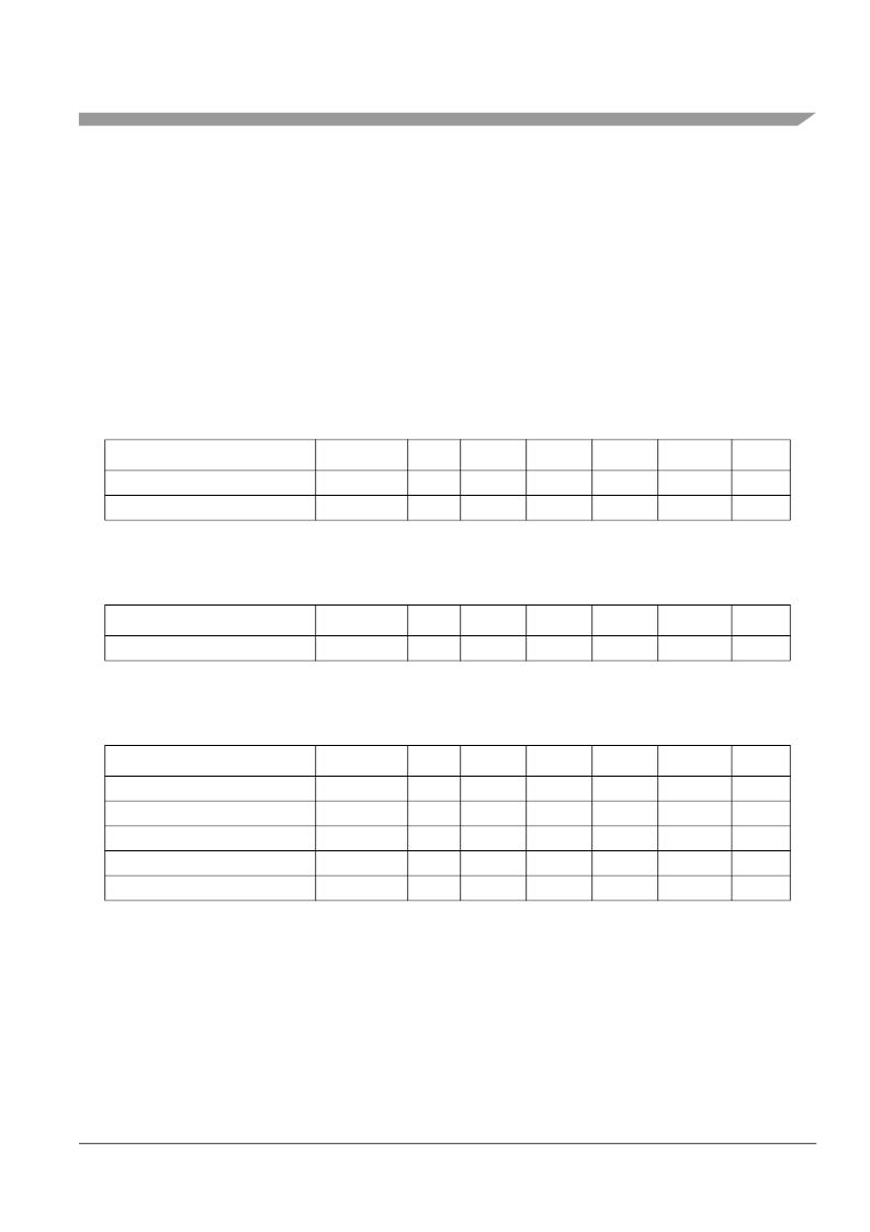
Table 8. System Oscillator Electrical Characteristics
Characteristic
Symbol
Notes
Min
Typical
Max
Unit
SpecID
SYS_XTAL frequency
f
sys_xtal
15.6
33.3
35.0
MHz
O1.1
Oscillator start-up time
t
up_osc
—
—
100
μ
s
O1.2
Table 9. RTC Oscillator Electrical Characteristics
Characteristic
Symbol
Notes
Min
Typical
Max
Unit
SpecID
RTC_XTAL frequency
f
rtc_xtal
—
32.768
—
kHz
O2.1
Table 10. System PLL Specifications
Characteristic
Symbol
Notes
Min
Typical
Max
Unit
SpecID
SYS_XTAL frequency
f
sys_xtal
1
NOTES:
1
The SYS_XTAL frequency and PLL Configuration bits must be chosen such that the resulting system frequency,
CPU (core) frequency, and PLL (VCO) frequency do not exceed their respective maximum or minimum operating
frequencies.
2
This represents total input jitter - short term and long term combined - and is guaranteed by design. Two different
types of jitter can exist on the input to core_sysclk, systemic and true random jitter. True random jitter is rejected, but
the PLL. Systemic jitter will be passed into and through the PLL to the internal clock circuitry, directly reducing the
operating frequency.
3
Relock time is guaranteed by design and characterization. PLL-relock time is the maximum amount of time required
for the PLL lock after a stable Vdd and core_sysclk are reached during the power-on reset sequence. This
specification also applies when the PLL has been disabled and subsequently re-enabled during sleep modes.
15.6
33.3
35.0
MHz
O3.1
SYS_XTAL cycle time
T
sys_xtal
(1)
66.6
30.0
28.5
ns
O3.2
SYS_XTAL clock input jitter
t
jitter
2
—
—
150
ps
O3.3
System VCO frequency
f
VCOsys
(1)
250
533
800
MHz
O3.4
System PLL relock time
t
lock
3
—
—
100
μ
s
O3.5
相關(guān)PDF資料 |
PDF描述 |
|---|---|
| MPC5534 | Microcontroller |
| MPC7447A | PowerPC microprocessor |
| MPC7447ANXPNS | PowerPC microprocessor |
| MPC7455 | RISC Microprocessor Hardware Specifications |
| MPC7457 | RISC Microprocessor Hardware Specifications |
相關(guān)代理商/技術(shù)參數(shù) |
參數(shù)描述 |
|---|---|
| MPC5200B | 制造商:FREESCALE 制造商全稱:Freescale Semiconductor, Inc 功能描述:SDRAM/DDR Memory Controller |
| MPC5200B_08 | 制造商:FREESCALE 制造商全稱:Freescale Semiconductor, Inc 功能描述:SDRAM / DDR Memory Controller |
| MPC5200B_10 | 制造商:FREESCALE 制造商全稱:Freescale Semiconductor, Inc 功能描述:SDRAM/DDR Memory Controller |
| MPC5200BDS | 制造商:FREESCALE 制造商全稱:Freescale Semiconductor, Inc 功能描述:Technical Data |
| MPC5200BV400 | 功能描述:微處理器 - MPU 400MHz 760MIPS RoHS:否 制造商:Atmel 處理器系列:SAMA5D31 核心:ARM Cortex A5 數(shù)據(jù)總線寬度:32 bit 最大時鐘頻率:536 MHz 程序存儲器大小:32 KB 數(shù)據(jù) RAM 大小:128 KB 接口類型:CAN, Ethernet, LIN, SPI,TWI, UART, USB 工作電源電壓:1.8 V to 3.3 V 最大工作溫度:+ 85 C 安裝風(fēng)格:SMD/SMT 封裝 / 箱體:FBGA-324 |
發(fā)布緊急采購,3分鐘左右您將得到回復(fù)。