- 您現(xiàn)在的位置:買賣IC網(wǎng) > PDF目錄371134 > MPC2605 (Motorola, Inc.) Integrated Secondary Cache for PowerPC Microprocessors PDF資料下載
參數(shù)資料
| 型號(hào): | MPC2605 |
| 廠商: | Motorola, Inc. |
| 英文描述: | Integrated Secondary Cache for PowerPC Microprocessors |
| 中文描述: | 綜合二級(jí)高速緩存的PowerPC微處理器 |
| 文件頁數(shù): | 3/30頁 |
| 文件大小: | 288K |
| 代理商: | MPC2605 |
第1頁第2頁當(dāng)前第3頁第4頁第5頁第6頁第7頁第8頁第9頁第10頁第11頁第12頁第13頁第14頁第15頁第16頁第17頁第18頁第19頁第20頁第21頁第22頁第23頁第24頁第25頁第26頁第27頁第28頁第29頁第30頁
MPC2605
3
MOTOROLA
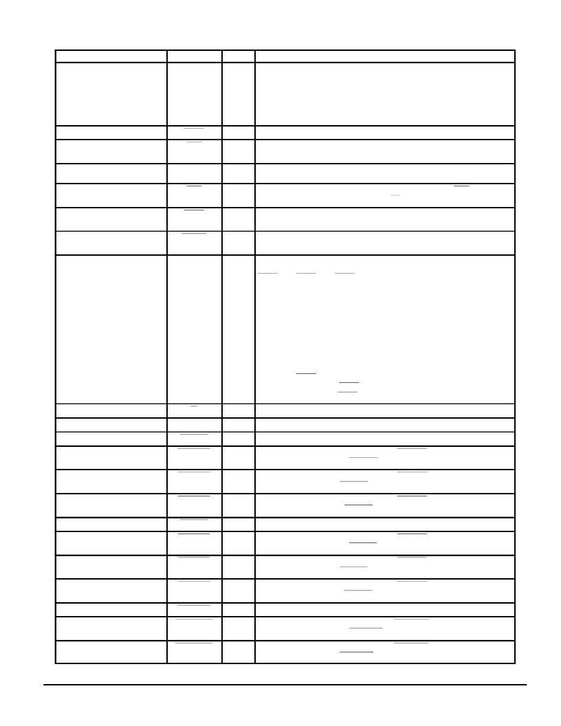
PIN DESCRIPTIONS
Pin Locations
Pin Name
Type
Description
19G, 17H – 19H, 17J – 19J,
17K – 19K, 17L – 19L,
17M – 19M, 17N – 19N,
17P – 19P, 17R – 19R,
18T, 19T, 18U, 19U,
18V, 19V, 18W
*
A0 – A31
I/O
Address inputs from processor. Can also be outputs for processor snoop
addresses. A0 is the MSB. A31 is the LSB.
3G
AACK
I/O
Address acknowledge input/output.
2A
ABB
I/O
Used as an input to qualify bus grants. Driven as an output during address tenure
initiated by the MPC2605.
17C – 19C, 17D
*
AP0 – AP3
I/O
Address parity.
19B
APE
O
Address parity error. When an address parity error is detected, APE will be driven
low one clock cycle after the assertion of TS then High–Z following clock cycle.
18E
APEN
I
Address parity enable. When tied low, enables address parity bits and the
address parity error bit.
1G
ARTRY
I/O
Address retry status I/O. Generated when a read or write snoop to a dirty
processor cache line has occurred.
2U
2V
1V
17E
2B
CFG0
CFG1
CFG2
CFG3
CFG4
I
Configuration inputs. These must be tied to either VDD or VSS.
CFG0
CFG1
CFG2
0
0
0
0
1
0
0
1
1
1
0
0
1
0
1
1
1
0
1
1
1
256KB
512KB; A26 = 0
512KB; A26 = 1
1MB; A25 – A26 = 00
1MB; A25 – A26 = 01
1MB; A25 – A26 = 10
1MB; A25 – A26 = 11
CFG3
Snoop Data Tenure Selector
0
Supports snoop data tenure
1
Does not support snoop data tenure
CFG4
AACK Driver Enable
0
Disable AACK driver
1
Enable AACK driver
2G
CI
I/O
Cache inhibit I/O.
3M
CLK
I
Clock input. This must be the same as the processor clock input.
2M
CPU BG
I
CPU bus grant input.
3E
CPU2 BG
I
MPC2605 logically ORs this signal with CPU BG. Used in multiprocessor
configuration as the second CPU BG.
1B
CPU3 BG
I
MPC2605 logically ORs this signal with CPU BG. Used in multiprocessor
configuration as the third CPU BG.
1T
CPU4 BG
I
MPC2605 logically ORs this signal with CPU BG. Used in multiprocessor
configuration as the fourth CPU BG.
2H
CPU BR
I
CPU bus request input.
2D
CPU2 BR
I
MPC2605 logically ORs this signal with CPU BR. Used in multiprocessor
configuration as the second CPU BR.
2C
CPU3 BR
I
MPC2605 logically ORs this signal with CPU BR. Used in multiprocessor
configuration as the third CPU BR.
1U
CPU4 BR
I
MPC2605 logically ORs this signal with CPU BR. Used in multiprocessor
configuration as the fourth CPU BR.
1F
CPU DBG
I
CPU data bus grant input from arbiter.
3D
CPU2 DBG
I
MPC2605 logically ORs this signal with CPU DBG. Used in multiprocessor
configuration as the second CPU DBG.
3C
CPU3 DBG
I
MPC2605 logically ORs this signal with CPU DBG. Used in multiprocessor
configuration as the third CPU DBG.
* See pin diagram (page 2) for specific pin assignment of these bus signals.
相關(guān)PDF資料 |
PDF描述 |
|---|---|
| MPC2605ZP66 | Circular Connector; Body Material:Aluminum; Series:PT07; Number of Contacts:36; Connector Shell Size:22; Connecting Termination:Solder; Circular Shell Style:Jam Nut Receptacle; Circular Contact Gender:Socket |
| MPC2605ZP66R | Integrated Secondary Cache for PowerPC Microprocessors |
| MPC500 | ELECTROHYDRAULIC BRAKING |
| MPC555D | This document provides an overview of the MPC555 microcontroller, including a block diagram showing the major modular components and sections that lis |
| MPC555PB | CABLE ASSEMBLY; ; NMO Antenna Mount to BNC Male, RG58C/U, 5 feet |
相關(guān)代理商/技術(shù)參數(shù) |
參數(shù)描述 |
|---|---|
| MPC2605ZP66 | 制造商:Motorola Inc 功能描述: 制造商:Motorola Inc 功能描述:CACHE SUBSYSTEM, 241 Pin, Plastic, BGA |
| MPC2605ZP66R | 制造商:MOTOROLA 制造商全稱:Motorola, Inc 功能描述:Integrated Secondary Cache for PowerPC Microprocessors |
| MPC2605ZP83 | 制造商:Rochester Electronics LLC 功能描述:- Bulk |
| MPC27T416TQ9 | 制造商:Motorola 功能描述:MOTOROLA |
| MPC-2C-24VDC | 制造商:Allied Controls Incorporated 功能描述: |
發(fā)布緊急采購,3分鐘左右您將得到回復(fù)。