- 您現(xiàn)在的位置:買賣IC網(wǎng) > PDF目錄371121 > MMBD3005T1 (MOTOROLA INC) SWITCHING DIODE PDF資料下載
參數(shù)資料
| 型號: | MMBD3005T1 |
| 廠商: | MOTOROLA INC |
| 元件分類: | 參考電壓二極管 |
| 英文描述: | SWITCHING DIODE |
| 中文描述: | 0.2 A, 2 ELEMENT, SILICON, SIGNAL DIODE |
| 文件頁數(shù): | 3/8頁 |
| 文件大?。?/td> | 160K |
| 代理商: | MMBD3005T1 |
3
Motorola Small–Signal Transistors, FETs and Diodes Device Data
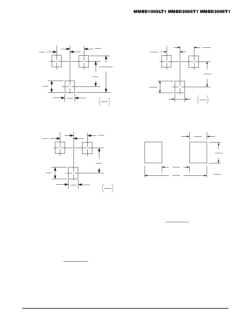
MINIMUM RECOMMENDED FOOTPRINT FOR SURFACE MOUNTED APPLICATIONS
Surface mount board layout is a critical portion of the total
design. The footprint for the semiconductor packages must
be the correct size to insure proper solder connection
interface between the board and the package. With the
correct pad geometry, the packages will self align when
subjected to a solder reflow process.
mm
inches
2.5-3.0
0.039
1.0
0.094
2.4
0.8
0.098-0.118
0.031
0.95
0.037
0.95
0.037
SOT–23
mm
inches
0.037
0.95
0.037
0.95
0.079
2.0
0.035
0.9
0.031
0.8
SC–59
mm
inches
0.035
0.9
0.075
0.7
1.9
0.028
0.65
0.025
0.65
0.025
SC–70/SOT–323
SOD–123
éééé
éééé
éééé
éééé
éééé
éééé
ééé
0.91
ééé
ééé
ééé
ééé
ééé
mm
inches
1.22
0.048
2.36
0.093
4.19
0.165
POWER DISSIPATION FOR A SURFACE MOUNT DEVICE
The power dissipation for a surface mount device is a
function of the drain/collector pad size. These can vary from
the minimum pad size for soldering to a pad size given for
maximum power dissipation. Power dissipation for a surface
mount device is determined by TJ(max), the maximum rated
junction temperature of the die, R
θ
JA, the thermal resistance
from the device junction to ambient, and the operating
temperature, TA. Using the values provided on the data
sheet, PD can be calculated as follows:
TJ(max) – TA
R
θ
JA
PD =
The values for the equation are found in the maximum
ratings table on the data sheet. Substituting these values into
the equation for an ambient temperature TA of 25
°
C, one can
calculate the power dissipation of the device. For example,
for a SOT–23 device, PD is calculated as follows.
PD =
150
°
C – 25
°
C
556
°
C/W
= 225 milliwatts
The 556
°
C/W for the SOT–23 package assumes the use
of the recommended footprint on a glass epoxy printed circuit
board to achieve a power dissipation of 250 milliwatts. There
are other alternatives to achieving higher power dissipation
from the surface mount packages. One is to increase the
area of the drain/collector pad. By increasing the area of the
drain/collector pad, the power dissipation can be increased.
Although the power dissipation can almost be doubled with
this method, area is taken up on the printed circuit board
which can defeat the purpose of using surface mount
technology.
Another alternative would be to use a ceramic substrate or
an aluminum core board such as Thermal Clad
. Using a
board material such as Thermal Clad, an aluminum core
board, the power dissipation can be doubled using the same
footprint.
相關(guān)PDF資料 |
PDF描述 |
|---|---|
| MMBD2005T1 | SWITCHING DIODE |
| MMBD110T1 | LED BLUE 465NM CLEAR SMD |
| MMBD770T1 | Schottky Barrier Diodes |
| MMBD330T1 | Schottky Barrier Diodes |
| MMBD110T1 | Schottky Barrier Diodes |
相關(guān)代理商/技術(shù)參數(shù) |
參數(shù)描述 |
|---|---|
| MMBD301 | 功能描述:肖特基二極管與整流器 RoHS:否 制造商:Skyworks Solutions, Inc. 產(chǎn)品:Schottky Diodes 峰值反向電壓:2 V 正向連續(xù)電流:50 mA 最大浪涌電流: 配置:Crossover Quad 恢復(fù)時間: 正向電壓下降:370 mV 最大反向漏泄電流: 最大功率耗散:75 mW 工作溫度范圍:- 65 C to + 150 C 安裝風(fēng)格:SMD/SMT 封裝 / 箱體:SOT-143 封裝:Reel |
| MMBD301L | 制造商:ONSEMI 制造商全稱:ON Semiconductor 功能描述:SILICON HOT-CARRIER DETECTOR AND SWITCHING DIODES |
| MMBD301LT1 | 功能描述:肖特基二極管與整流器 30V 200mW Single RoHS:否 制造商:Skyworks Solutions, Inc. 產(chǎn)品:Schottky Diodes 峰值反向電壓:2 V 正向連續(xù)電流:50 mA 最大浪涌電流: 配置:Crossover Quad 恢復(fù)時間: 正向電壓下降:370 mV 最大反向漏泄電流: 最大功率耗散:75 mW 工作溫度范圍:- 65 C to + 150 C 安裝風(fēng)格:SMD/SMT 封裝 / 箱體:SOT-143 封裝:Reel |
| MMBD301LT1G | 功能描述:肖特基二極管與整流器 30V 200mW Single RoHS:否 制造商:Skyworks Solutions, Inc. 產(chǎn)品:Schottky Diodes 峰值反向電壓:2 V 正向連續(xù)電流:50 mA 最大浪涌電流: 配置:Crossover Quad 恢復(fù)時間: 正向電壓下降:370 mV 最大反向漏泄電流: 最大功率耗散:75 mW 工作溫度范圍:- 65 C to + 150 C 安裝風(fēng)格:SMD/SMT 封裝 / 箱體:SOT-143 封裝:Reel |
| MMBD301LT3 | 功能描述:肖特基二極管與整流器 30V 200mW Single RoHS:否 制造商:Skyworks Solutions, Inc. 產(chǎn)品:Schottky Diodes 峰值反向電壓:2 V 正向連續(xù)電流:50 mA 最大浪涌電流: 配置:Crossover Quad 恢復(fù)時間: 正向電壓下降:370 mV 最大反向漏泄電流: 最大功率耗散:75 mW 工作溫度范圍:- 65 C to + 150 C 安裝風(fēng)格:SMD/SMT 封裝 / 箱體:SOT-143 封裝:Reel |
發(fā)布緊急采購,3分鐘左右您將得到回復(fù)。