- 您現(xiàn)在的位置:買賣IC網 > PDF目錄382330 > MM54C221 (National Semiconductor Corporation) Dual Monostable Multivibrator PDF資料下載
參數(shù)資料
| 型號: | MM54C221 |
| 廠商: | National Semiconductor Corporation |
| 英文描述: | Dual Monostable Multivibrator |
| 中文描述: | 雙單穩(wěn)態(tài)觸發(fā)器 |
| 文件頁數(shù): | 3/6頁 |
| 文件大小: | 148K |
| 代理商: | MM54C221 |
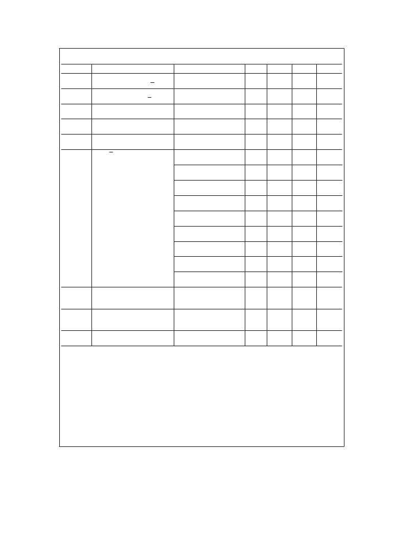
AC Electrical Characteristics
*
T
A
e
25
§
C, C
L
e
50 pF, unless otherwise noted
Symbol
Parameter
Conditions
Min
Typ
Max
Units
t
pd A, B
Propagation Delay from Trigger
Input (A, B) to Output Q, Q
V
CC
e
5V
V
CC
e
10V
250
120
500
250
ns
ns
t
pd CL
Propagation Delay from Clear
Input (CL) to Output Q, Q
V
CC
e
5V
V
CC
e
10V
250
120
500
250
ns
ns
t
S
Time Prior to Trigger Input (A, B)
that Clear must be Set
V
CC
e
5V
V
CC
e
10V
150
60
50
20
ns
ns
t
W(A, B)
Trigger Input (A, B) Pulse Width
V
CC
e
5V
V
CC
e
10V
150
70
50
30
ns
ns
t
W(CL)
Clear Input (CL) Pulse Width
V
CC
e
5V
V
CC
e
10V
150
70
50
30
ns
ns
t
W(OUT)
Q or Q Output Pulse Width
V
CC
e
5V, R
EXT
e
10k,
C
EXT
e
0 pF
900
ns
V
CC
e
10V, R
EXT
e
10k,
C
EXT
e
0 pF
350
ns
V
CC
e
15V, R
EXT
e
10k,
C
EXT
e
0 pF
320
ns
V
CC
e
5V, R
EXT
e
10k,
C
EXT
e
1000 pF(Figure 1)
9.0
10.6
12.2
m
s
V
CC
e
10V, R
EXT
e
10k,
C
EXT
e
1000 pF(Figure 1)
9.0
10
11
m
s
V
CC
e
15V, R
EXT
e
10k,
C
EXT
e
1000 pF(Figure 1)
8.9
9.8
10.8
m
s
V
CC
e
5V, R
EXT
e
10k,
C
EXT
e
0.1
m
F(Figure 2)
900
1020
1200
m
s
V
CC
e
10V, R
EXT
e
10k,
C
EXT
e
0.1
m
F(Figure 2)
900
1000
1100
m
s
V
CC
e
15V, R
EXT
e
10k,
C
EXT
e
0.1
m
F(Figure 2)
900
990
1100
m
s
R
ON
ON Resistance of Transistor
between R/C
EXT
to C
EXT
V
CC
e
5V (Note 4)
V
CC
e
10V (Note 4)
V
CC
e
15V (Note 4)
50
25
16.7
150
65
45
X
X
X
Output Duty Cycle
R
e
10k, C
e
1000 pF
R
e
10k, C
e
0.1
m
F
(Note 5)
90
90
%
%
C
IN
Input Capacitance
R/C
EXT
Input (Note 2)
Any Other Input (Note 2)
15
5
25
pF
pF
*
AC Parameters are guaranteed by DC correlated testing.
Note 1:
‘‘Absolute Maximum Ratings’’ are those values beyond which the safety of the device cannot be guaranteed. Except for ‘‘Operating Temperature Range’’
they are not meant to imply that the devices should be operated at these limits. The table of ‘‘Electrical Characteristics’’ provides conditions for actual device
operation.
Note 2:
Capacitance is guaranteed by periodic testing.
Note 3:
In Standby (Q
e
Logic ‘‘0’’) the power dissipated equals the leakage current plus V
CC
/R
EXT
.
Note 4:
See AN-138 for detailed explanation R
ON
.
Note 5:
Maximum output duty cycle
e
R
EXT
/R
EXT
a
1000.
3
相關PDF資料 |
PDF描述 |
|---|---|
| MM54C221J | Dual Monostable Multivibrator |
| MM54C221N | Dual Monostable Multivibrator |
| MM54C240 | Octal Buffers and Line Drivers with TRI-STATE Outputs |
| MM54C240J | Octal Buffers and Line Drivers with TRI-STATE Outputs |
| MM54C240N | Octal Buffers and Line Drivers with TRI-STATE Outputs |
相關代理商/技術參數(shù) |
參數(shù)描述 |
|---|---|
| MM54C221 WAF | 制造商:Texas Instruments 功能描述: |
| MM54C221J | 制造商:NSC 制造商全稱:National Semiconductor 功能描述:Dual Monostable Multivibrator |
| MM54C221J/883 | 制造商:National Semiconductor Corporation 功能描述:Monostable Multivibrator Dual |
| MM54C221N | 制造商:NSC 制造商全稱:National Semiconductor 功能描述:Dual Monostable Multivibrator |
| MM54C221W/883 | 制造商:Rochester Electronics LLC 功能描述:- Bulk 制造商:Texas Instruments 功能描述: |
發(fā)布緊急采購,3分鐘左右您將得到回復。