- 您現(xiàn)在的位置:買(mǎi)賣(mài)IC網(wǎng) > PDF目錄383618 > MK53761 (意法半導(dǎo)體) REPERTORY DIALER PDF資料下載
參數(shù)資料
| 型號(hào): | MK53761 |
| 廠(chǎng)商: | 意法半導(dǎo)體 |
| 英文描述: | REPERTORY DIALER |
| 中文描述: | 劇目撥號(hào)器 |
| 文件頁(yè)數(shù): | 2/11頁(yè) |
| 文件大小: | 199K |
| 代理商: | MK53761 |
FUNCTIONAL PIN DESCRIPTION (DIP18 only)
V+
Pin 1. V+ is the positive supply for the circuit and
must meet themaximum andminimum voltage re-
quirements.(see electrical specifications).
MODE
Input.Pin 2. MODE determines the dialer’s default
operatingmode. When the deviceis poweredupor
thehookswitchinputis switchedfromon-hook,(V+),
to off-hook,(V–), the defaultdeterminesthe signal-
ing mode. A V+ connection defaults to tone mode
operation and a V– connection defaults to pulse
mode operation.
Whendialinginthepulsemode,asoftswitchfeature
will allow a changeto thetonemode wheneverthe
* key,orsoftswitch,isdepressed.Subsequent*key
inputswill causetheDTMFcodeforan*tobedialed.
Thesoftswitchwillonlyswitchfrompulsetotone.Af-
ter returning to on-hook and back to off-hook, the
partwillbeinpulsemode.RedialbytheLND keywill
repeat thesoftswitch.
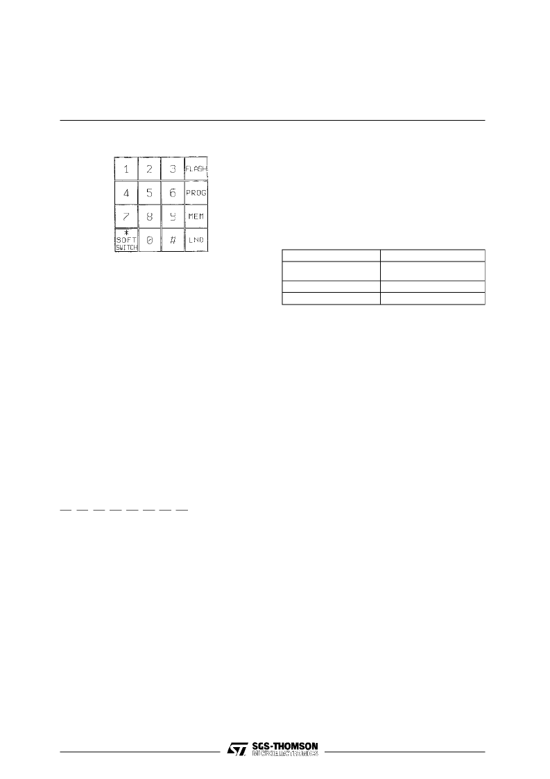
C1, C2, C3, C4, R4, R3, R2, R1
Keyboard inputs. The MK53761 interfaces with
either thestandard2-of-8 with negativecommon or
the singlecontact(Form A) keyboard.
A valid keypad entry is either a single Row con-
nectedtoasingleColumnorV–simultaneouslypre-
sentedto both asingle Row and Column. In its qui-
escentorstandbystate, during normal off-hookop-
eration, either the Rows or the Columns are at a
logic level 1 (V+). Pulling one inputlow enablesthe
on-chip oscillator.Keyboard scanningthen begins.
ScanningconsistsofRowsandColumnsalternately
switching highthroughon-chippullups.Afterboth a
Row and Column keyhave been detected,thede-
bouncecounterisenabledandanynoise(bouncing
contacts, etc.) is ignored for a debounce period
(TK
D
) of32ms.Atthistime,thekeyboardissampled
and if bothRow and Column informationare valid,
the information is bufferedinto the LND location. If
switchedon-hook(pin 17to pin 1), thekeyboardin-
putsall pull high through on-chippullup resistors.
Figure2
: KeypadConfiguration.
In thetonemode, if 2 or more keysin thesamerow
or if 2 or more keys in the same column are de-
pressed a single tone will be output. The tone will
corres-pond to the row or column for which the 2
keyswerepushed.Thisfeatureis fortest purposes,
and single toneswill notbe redialed.
Alsointhetonemode,theoutputtoneiscontinuous
is manualdialingaslong as thekeyis pushed.The
outputtone durationfollows the table1.
Table 1 :
OutputToneDuration.
Key-Push Time, T*
T
≤
32ms
Tone Output*
No Output Ignored by
MK53761
75ms Duration Output
Output Duration = T – T
KD
32ms
≤
T
≤
75ms + T
KD
T
≥
75ms + T
KD
* TKD is the key pad debounce time which is typically 32 ms.
Whenredialinginthetonemode,eachDTMFoutput
is 75ms duration,and the tone separation(intersig-
nal delay) is 50ms.
V–
Input. Pin 6 is the negativesupply input to the de-
vice. This is the voltage referencefor all specifica-
tions.
OSC1, OSC2
Pin 7 (input), pin 8 (output).OSC1 and OSC2 are
connectionsto an on-chipinverter used as the tim-
ingreferenceforthecircuit. Ithassufficientloopgain
to oscillate when used with a low-cost television
color-burstcrystal. Thenominalcrystal frequencyis
3.579545MHz andanydeviationfrom thisstandard
is directly reflected in the Tone outputfrequencies.
Thecrystaloscillatorprovidesthetime referencefor
all circuit functions.A ceramic resonatorwith toler-
ance of
±
0.25% may also be used.
DTMF OUTPUT
Output.Pin10.AnNPNtransistoremitterwithacol-
lectortiedto V+drivestheDTMF OUTPUT pin.The
transistor base is connected to an on-chip opera-
tional amplifier that mixes the Row and Column
tones.Figure 7 shows thetiming at this pin.
The DTMF OUTPUT is the summation of a single
Row frequency and a singleColumn frequency. A
typical single tone sine wave is shown in Figure 4.
This waveform is synthesized using a resistor tree
withsinusoidally weighted taps.
The MK53761 is designed to operate from an un-
regulatedsupply; theTONE LEVELis supply inde-
pendent,andthesinglerowtoneoutputlevelwill be
typically :
T
oi
= –12 dBm
±
1 dB
TheDC componentof theDTMFoutputwhileactive
is describedby the following equation:
VDC
1
= 0.3 V+ + 0.5 Volts
MK53761
2/11
相關(guān)PDF資料 |
PDF描述 |
|---|---|
| MK53761D | REPERTORY DIALER |
| MK53761N00 | REPERTORY DIALER |
| MKP1837 | Metallized Polypropylene Film Capacitor |
| MKP1837-322-162 | Metallized Polypropylene Film Capacitor |
| MKP1837-322-162-D | Metallized Polypropylene Film Capacitor |
相關(guān)代理商/技術(shù)參數(shù) |
參數(shù)描述 |
|---|---|
| MK53761D | 制造商:STMICROELECTRONICS 制造商全稱(chēng):STMicroelectronics 功能描述:REPERTORY DIALER |
| MK53761N00 | 制造商:STMICROELECTRONICS 制造商全稱(chēng):STMicroelectronics 功能描述:REPERTORY DIALER |
| MK53DN512CLQ10 | 功能描述:ARM微控制器 - MCU KINETIS 512K RoHS:否 制造商:STMicroelectronics 核心:ARM Cortex M4F 處理器系列:STM32F373xx 數(shù)據(jù)總線(xiàn)寬度:32 bit 最大時(shí)鐘頻率:72 MHz 程序存儲(chǔ)器大小:256 KB 數(shù)據(jù) RAM 大小:32 KB 片上 ADC:Yes 工作電源電壓:1.65 V to 3.6 V, 2 V to 3.6 V, 2.2 V to 3.6 V 工作溫度范圍:- 40 C to + 85 C 封裝 / 箱體:LQFP-48 安裝風(fēng)格:SMD/SMT |
| MK53DN512CMD10 | 制造商:Freescale Semiconductor 功能描述:KINETIS K 32-BIT MCU, ARM CORTEX-M4 CORE, 512KB FLASH, 100MH - Bulk 制造商:Freescale Semiconductor 功能描述:IC MCU ARM 512KB FLASH 144BGA 制造商:Freescale Semiconductor 功能描述:MCU 32BIT KINETIS 512K 144MAP 制造商:Freescale Semiconductor 功能描述:MCU, 32BIT, KINETIS, 512K, 144MAP 制造商:Freescale Semiconductor 功能描述:ARM Microcontrollers - MCU KINETIS 512K MED LCD ENE 制造商:Freescale Semiconductor 功能描述:MCU, 32BIT, KINETIS, 512K, 144MAP, Controller Family/Series:(ARM Cortex - M4) Ki 制造商:Freescale Semiconductor 功能描述:KINETIS 512K MED LCD ENE |
| MK53DN512ZCLQ10 | 功能描述:ARM微控制器 - MCU KINETIS 512K SLCD+ETHNET RoHS:否 制造商:STMicroelectronics 核心:ARM Cortex M4F 處理器系列:STM32F373xx 數(shù)據(jù)總線(xiàn)寬度:32 bit 最大時(shí)鐘頻率:72 MHz 程序存儲(chǔ)器大小:256 KB 數(shù)據(jù) RAM 大小:32 KB 片上 ADC:Yes 工作電源電壓:1.65 V to 3.6 V, 2 V to 3.6 V, 2.2 V to 3.6 V 工作溫度范圍:- 40 C to + 85 C 封裝 / 箱體:LQFP-48 安裝風(fēng)格:SMD/SMT |
發(fā)布緊急采購(gòu),3分鐘左右您將得到回復(fù)。