- 您現(xiàn)在的位置:買賣IC網(wǎng) > PDF目錄371115 > MJE13007 (Electronic Theatre Controls, Inc.) Mini size of Discrete semiconductor elements PDF資料下載
參數(shù)資料
| 型號: | MJE13007 |
| 廠商: | Electronic Theatre Controls, Inc. |
| 英文描述: | Mini size of Discrete semiconductor elements |
| 中文描述: | 迷你型離散半導體元件 |
| 文件頁數(shù): | 6/10頁 |
| 文件大小: | 337K |
| 代理商: | MJE13007 |
6
Motorola Bipolar Power Transistor Device Data
T
t1 ADJUSTED TO
OBTAIN IC
Lcoil (ICM)
TEST EQUIPMENT
SCOPE — TEKTRONIX
475 OR EQUIVALENT
t1
≈
VCC
Lcoil (ICM)
Vclamp
t2
≈
C
V
VCC = 125 V
RC = 25
D1 = 1N5820 OR EQUIV.
T
REVERSE BIAS SAFE OPERATING AREA AND INDUCTIVE SWITCHING
RESISTIVE
SWITCHING
Table 1. Test Conditions For Dynamic Performance
L = 10 mH
RB2 = 8
VCC = 20 Volts
IC(pk) = 100 mA
L = 200 mH
RB2 = 0
VCC = 15 Volts
RB1 selected for
desired IB1
L = 500 mH
RB2 = 0
VCC = 15 Volts
RB1 selected for
desired IB1
V(BR)CEO(sus)
Inductive
Switching
RBSOA
TYPICAL
WAVEFORMS
VCC
L
MUR8100E
Vclamp = 300 Vdc
VCE
51
5.1 k
TUT
IB
IC
+15 V
+10 V
50
RB1
RB2
150
3 W
500
μ
F
1
μ
F
A
100
μ
F
Voff
COMMON
MTP8P10
MTP12N10
MPF930
MPF930
MTP8P10
MJE210
IB
MUR105
1
μ
F
100
3 W
150
3 W
+125
V
SCOPE
RC
TUT
D1
RB
– 4 V
IC
VCE
ICM
t1
tf
t
t
Vclamp
t2
TIME
VCEM
tf CLAMPED
tf UNCLAMPED
≈
t2
25
μ
s
+11 V
0
9 V
DUTtr, tf < 10 ns
RB AND RC ADJUSTED
FOR DESIRED IB AND IC
VCE
VCE PEAK
IB
IB2
IB1
VOLTAGE REQUIREMENTS
(continued)
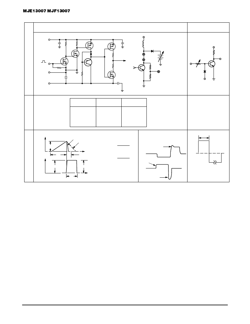
In the four application examples (Table 2) load lines are
shown in relation to the pulsed forward and reverse biased
SOA curves.
In circuits A and D, inductive reactance is clamped by the
diodes shown. In circuits B and C the voltage is clamped by
the output rectifiers, however, the voltage induced in the pri-
mary leakage inductance is not clamped by these diodes and
could be large enough to destroy the device. A snubber net-
work or an additional clamp may be required to keep the
turn–off load line within the Reverse Bias SOA curve.
Load lines that fall within the pulsed forward biased SOA
curve during turn–on and within the reverse bias SOA curve
during turn–off are considered safe, with the following as-
sumptions:
(1) The device thermal limitations are not exceeded.
(2) The turn–on time does not exceed 10
μ
s (see standard
pulsed forward SOA curves in Figure 6).
(3) The base drive conditions are within the specified limits
shown on the Reverse Bias SOA curve (Figure 7).
CURRENT REQUIREMENTS
An efficient switching transistor must operate at the re-
quired current level with good fall time, high energy handling
capability and low saturation voltage. On this data sheet,
these parameters have been specified at 5.0 amperes which
represents typical design conditions for these devices. The
current drive requirements are usually dictated by the
VCE(sat) specification because the maximum saturation volt-
age is specified at a forced gain condition which must be du-
plicated or exceeded in the application to control the
saturation voltage.
SWITCHING REQUIREMENTS
In many switching applications, a major portion of the
transistor power dissipation occurs during the fall time (tfi).
For this reason considerable effort is usually devoted to
reducing the fall time. The recommended way to accomplish
this is to reverse bias the base–emitter junction during turn–
off. The reverse biased switching characteristics for inductive
loads are shown in Figures 13 and 14 and resistive loads in
Figures 11 and 12. Usually the inductive load components
will be the dominant factor in SWITCHMODE applications
and the inductive switching data will more closely represent
the device performance in actual application. The inductive
switching characteristics are derived from the same circuit
used to specify the reverse biased SOA curves, (see Table 1)
providing correlation between test procedures and actual
use conditions.
相關PDF資料 |
PDF描述 |
|---|---|
| MJE13007R | Mini size of Discrete semiconductor elements |
| MJE13007 | POWER TRANSISTOR |
| MJF13007 | POWER TRANSISTOR |
| MJF13007 | POWER TRANSISTOR 8.0 AMPERES 400 VOLTS 80/40 WATTS |
| MJE13007 | High Voltage Switch Mode Application |
相關代理商/技術參數(shù) |
參數(shù)描述 |
|---|---|
| MJE13007_06 | 制造商:KEC 制造商全稱:KEC(Korea Electronics) 功能描述:TO-220AB PACKAGE |
| MJE13007_08 | 制造商:KEC 制造商全稱:KEC(Korea Electronics) 功能描述:TRIPLE DIFFUSED NPN TRANSISTOR |
| MJE13007_10 | 制造商:UTC-IC 制造商全稱:UTC-IC 功能描述:NPN BIPOLAR POWER TRANSISTOR FOR SWITCHING POWER SUPPLY APPLICATIONS |
| MJE13007A | 功能描述:兩極晶體管 - BJT NPN Hi-Volt Fast Sw RoHS:否 制造商:STMicroelectronics 配置: 晶體管極性:PNP 集電極—基極電壓 VCBO: 集電極—發(fā)射極最大電壓 VCEO:- 40 V 發(fā)射極 - 基極電壓 VEBO:- 6 V 集電極—射極飽和電壓: 最大直流電集電極電流: 增益帶寬產(chǎn)品fT: 直流集電極/Base Gain hfe Min:100 A 最大工作溫度: 安裝風格:SMD/SMT 封裝 / 箱體:PowerFLAT 2 x 2 |
| MJE13007D | 制造商:UTC-IC 制造商全稱:UTC-IC 功能描述:NPN BIPOLAR POWER TRANSISTOR FOR SWITCHING POWER SUPPLY APPLICATIONS |
發(fā)布緊急采購,3分鐘左右您將得到回復。