- 您現(xiàn)在的位置:買賣IC網(wǎng) > PDF目錄382324 > MF6CWM-100 (NATIONAL SEMICONDUCTOR CORP) 6th Order Switched Capacitor Butterworth Lowpass PDF資料下載
參數(shù)資料
| 型號: | MF6CWM-100 |
| 廠商: | NATIONAL SEMICONDUCTOR CORP |
| 元件分類: | 運(yùn)動(dòng)控制電子 |
| 英文描述: | 6th Order Switched Capacitor Butterworth Lowpass |
| 中文描述: | SWITCHED CAPACITOR FILTER, BUTTERWORTH, LOWPASS, PDSO14 |
| 封裝: | SO-14 |
| 文件頁數(shù): | 4/20頁 |
| 文件大小: | 861K |
| 代理商: | MF6CWM-100 |

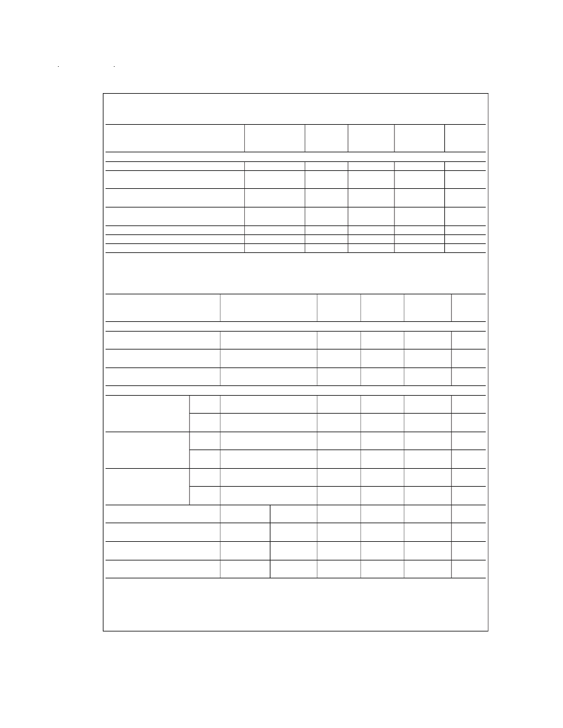
Op Amp Electrical Characteristics
(Continued)
Boldface limits apply for T
MIN
to T
MAX
;
all other limits T
A
= T
J
= 25C.
Parameter
Conditions
Typical
(Note 8)
Tested
Limit
(Note 9)
Design
Limit
(Note 10)
Units
V
+
= +2.5V, V
= 2.5V
Input Bias Current
CMRR (Op-Amp
#
2 Only)
10
60
pA
dB
V
CM1
= +0.5V,
V
CM2
= 0.9V
R
L
= 10 k
55
Output Voltage Swing
+1.5
2.2
24
1.0
6.0
67
1.2
+1.3
1.7
+1.1
1.7
V
Maximum Output Short
Circuit Current (Note 6)
Slew Rate
DC Open Loop Gain
Gain Bandwidth Product
Source
Sink
mA
V/μs
dB
MHz
Logic Input-Output Electrical Characteristics
(Note 5) The following specifications apply for V
= 0V unless otherwise specified.
Boldface limits apply for T
MIN
to
T
MAX
;
all other limits T
A
= T
J
= 25C.
Parameter
Conditions
Typical
(Note 8)
Tested
Limit
(Note 9)
Design
Limit
(Note 10)
Units
TTL CLOCK INPUT, CLK R PIN
(Note 7)
Maximum V
IL
, Logical “0”
Input Voltage
Minimum V
IH
, Logical “1”
Input Voltage
Maximum Leakage Current
at CLK R Pin
SCHMITT TRIGGER
V
T+
, Positive Going
Threshold Voltage
0.8
0.8
V
2.0
2.0
V
L Sh Pin at
Mid- Supply
2.0
2.0
μA
Min
Max
Min
Max
Min
Max
Min
Max
Min
Max
Min
Max
V
+
= 10V
7.0
6.1
8.9
3.1
4.4
1.3
3.8
0.6
1.9
2.3
7.6
1.2
3.8
9.0
4.5
1.0
0.5
3.0
0.75
2.5
0.65
6.1
8.9
3.1
4.4
1.3
3.8
0.6
1.9
2.3
7.6
1.2
3.8
9.0
4.5
1.0
0.5
3.0
0.75
2.5
0.65
V
V
+
= 5V
3.5
V
V
T
, Negative Going
Threshold Voltage
V
+
= 10V
3.0
V
V
+
= 5V
1.5
V
Hysteresis (V
T+
V
T
)
V
+
= 10V
4.0
V
V
+
= 5V
2.0
V
Minimum Logical “1” Output
Voltage (Pin 11)
Maximum Logical “0” Output
Voltage (Pin 11)
Minimum Output Source
Current (Pin 11)
Maximum Output Sink
Current (Pin 11)
I
o
= 10μA
V
+
= 10V
V
+
= 5V
V
+
= 10V
V
+
= 5V
V
+
= 10V
V
+
= 5V
V
+
= 10V
V
+
= 5V
V
I
o
= 10μA
V
CLK R Tied
to Ground
CLK R Tied
to V
+
6.0
1.5
5.0
1.3
mA
mA
Note 1:
The cutoff frequency of the filter is defined as the frequency where the magnitude response is 3.01 dB less than the DC gain of the filter.
Note 2:
For
±
5V supplies the dynamic range is referenced to 2.82 Vrms (4V peak) where the wideband noise over a 20 kHz bandwidth is typically 200 μVrms for
the MF6-50 and 250 μVrms for the MF6-100. For
±
2.5V supplies the dynamic range is referenced to 1.06 Vrms (1.5V peak) where the wideband noise over a 20 kHz
bandwidth is typically 140 μVrms for both the MF6-50 and the MF6-100.
Note 3:
The specifications for the MF6 have been given for a clock frequency (f
) of 250 kHz and less. Above this clock frequency the cutoff frequency begins to
deviate from the specified error band of
±
1.0% but the filter still maintains its magnitude characteristics. See Application Hints, Section 1.5.
www.national.com
4
相關(guān)PDF資料 |
PDF描述 |
|---|---|
| MF6CWM-50 | 6th Order Switched Capacitor Butterworth Lowpass |
| MF6C | ORDER SWITCHED CAPACITOR BUTTERWORTH LOWPASS FILTER |
| MF6 | 6th Order Switched Capacitor Butterworth Lowpass |
| MFE1842BBU22 | Dielectric Filter with Attenuation Pole |
| MG-12232-3 | LCD MODULE |
相關(guān)代理商/技術(shù)參數(shù) |
參數(shù)描述 |
|---|---|
| MF6CWM-50 | 制造商:NSC 制造商全稱:National Semiconductor 功能描述:6th Order Switched Capacitor Butterworth Lowpass |
| MF6M | 制造商:GOOD-ARK 制造商全稱:GOOD-ARK Electronics 功能描述:Miniature Glass Passivated Single-Phase Bridge Rectifiers |
| MF6S | 制造商:GOOD-ARK 制造商全稱:GOOD-ARK Electronics 功能描述:Miniature Glass Passivated Single-Phase Bridge Rectifiers |
| MF-7 | 制造商:Velleman Inc 功能描述:Conn Power Adapter M/F 2/2 POS ST 1 Port Bulk |
| MF70 | 制造商:DYNEX 制造商全稱:Dynex Semiconductor 功能描述:Fast Recovery Diode |
發(fā)布緊急采購,3分鐘左右您將得到回復(fù)。