- 您現(xiàn)在的位置:買賣IC網(wǎng) > PDF目錄45323 > MF280C51T-20R (ATMEL CORP) 8-BIT, MROM, 20 MHz, MICROCONTROLLER, PQFP44 PDF資料下載
參數(shù)資料
| 型號: | MF280C51T-20R |
| 廠商: | ATMEL CORP |
| 元件分類: | 微控制器/微處理器 |
| 英文描述: | 8-BIT, MROM, 20 MHz, MICROCONTROLLER, PQFP44 |
| 封裝: | QFP-44 |
| 文件頁數(shù): | 150/170頁 |
| 文件大小: | 4133K |
| 代理商: | MF280C51T-20R |
第1頁第2頁第3頁第4頁第5頁第6頁第7頁第8頁第9頁第10頁第11頁第12頁第13頁第14頁第15頁第16頁第17頁第18頁第19頁第20頁第21頁第22頁第23頁第24頁第25頁第26頁第27頁第28頁第29頁第30頁第31頁第32頁第33頁第34頁第35頁第36頁第37頁第38頁第39頁第40頁第41頁第42頁第43頁第44頁第45頁第46頁第47頁第48頁第49頁第50頁第51頁第52頁第53頁第54頁第55頁第56頁第57頁第58頁第59頁第60頁第61頁第62頁第63頁第64頁第65頁第66頁第67頁第68頁第69頁第70頁第71頁第72頁第73頁第74頁第75頁第76頁第77頁第78頁第79頁第80頁第81頁第82頁第83頁第84頁第85頁第86頁第87頁第88頁第89頁第90頁第91頁第92頁第93頁第94頁第95頁第96頁第97頁第98頁第99頁第100頁第101頁第102頁第103頁第104頁第105頁第106頁第107頁第108頁第109頁第110頁第111頁第112頁第113頁第114頁第115頁第116頁第117頁第118頁第119頁第120頁第121頁第122頁第123頁第124頁第125頁第126頁第127頁第128頁第129頁第130頁第131頁第132頁第133頁第134頁第135頁第136頁第137頁第138頁第139頁第140頁第141頁第142頁第143頁第144頁第145頁第146頁第147頁第148頁第149頁當(dāng)前第150頁第151頁第152頁第153頁第154頁第155頁第156頁第157頁第158頁第159頁第160頁第161頁第162頁第163頁第164頁第165頁第166頁第167頁第168頁第169頁第170頁
80
ATtiny4/5/9/10 [DATASHEET]
8127F–AVR–02/2013
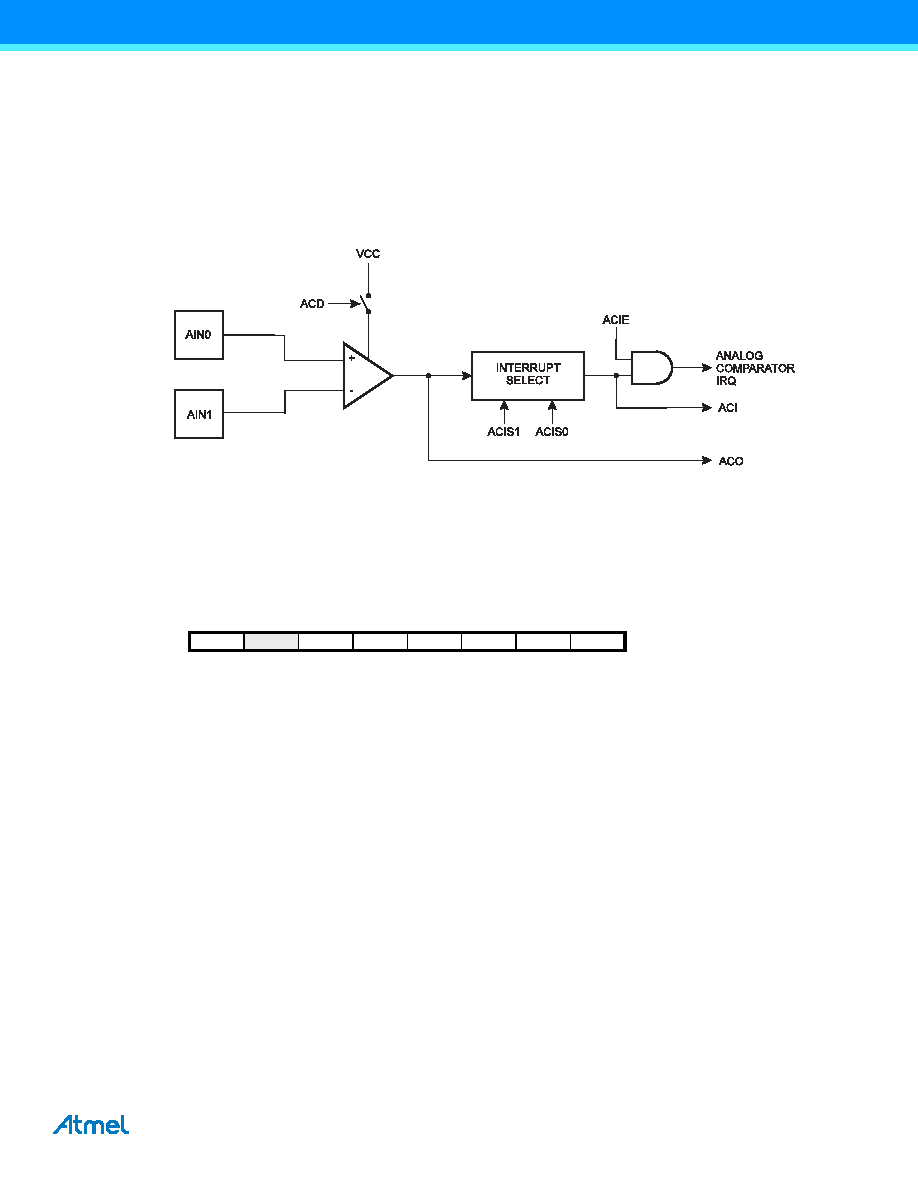
12. Analog Comparator
The Analog Comparator compares the input values on the positive pin AIN0 and negative pin AIN1. When the volt-
age on the positive pin AIN0 is higher than the voltage on the negative pin AIN1, the Analog Comparator output,
ACO, is set. The comparator can trigger a separate interrupt, exclusive to the Analog Comparator. The user can
select Interrupt triggering on comparator output rise, fall or toggle. A block diagram of the comparator and its sur-
rounding logic is shown in Figure 12-1.
Figure 12-1. Analog Comparator Block Diagram.
See Figure 1-1 on page 2 for pin use of analog comparator, and Table 10-4 on page 49 and Table 10-5 on page 50
for alternate pin usage.
12.1
Register Description
12.1.1
ACSR – Analog Comparator Control and Status Register
Bit 7 – ACD: Analog Comparator Disable
When this bit is written logic one, the power to the analog comparator is switched off. This bit can be set at any time
to turn off the analog comparator, thus reducing power consumption in Active and Idle mode. When changing the
ACD bit, the analog comparator Interrupt must be disabled by clearing the ACIE bit in ACSR. Otherwise an inter-
rupt can occur when the bit is changed.
Bits 6 – Res: Reserved Bit
This bit is reserved and will always read zero.
Bit 5 – ACO: Analog Comparator Output
Enables output of analog comparator. The output of the analog comparator is synchronized and then directly con-
nected to ACO. The synchronization introduces a delay of 1 - 2 clock cycles.
Bit
765
4321
0
ACD
–
ACO
ACI
ACIE
ACIC
ACIS1
ACIS0
ACSR
Read/Write
R/W
R
R/W
Initial Value
000
0000
0
發(fā)布緊急采購,3分鐘左右您將得到回復(fù)。