- 您現(xiàn)在的位置:買賣IC網(wǎng) > PDF目錄371098 > MF-2500DS-T12-191 (Mitsubishi Electric Corporation) SONET/SDH TRANSMITTER & RECIEVER PDF資料下載
參數(shù)資料
| 型號(hào): | MF-2500DS-T12-191 |
| 廠商: | Mitsubishi Electric Corporation |
| 英文描述: | SONET/SDH TRANSMITTER & RECIEVER |
| 中文描述: | SONET / SDH的變送器 |
| 文件頁(yè)數(shù): | 5/9頁(yè) |
| 文件大?。?/td> | 57K |
| 代理商: | MF-2500DS-T12-191 |
MITSUBISHI (OPTICAL DEVICES)
MF-2500DS-T12-18x/19x/20x/21x
MF-2500DS-R13-18x
MF-2500DS-R14-19x/20x/21x
SONET/SDH TRANSMITTER & RECIEVER
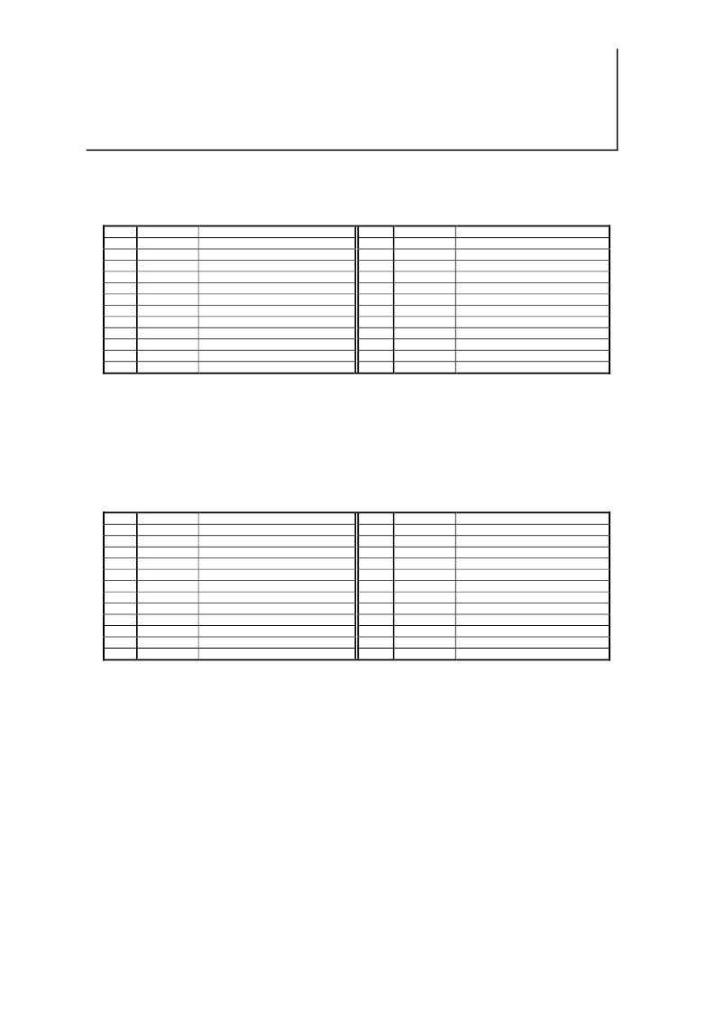
PIN ALLOCATION
Transmitter pin allocation
No.
1
2
3
4
5
6
7
8
9
10
11
12
Symbol
VEE
BACK(+)
BIAS(+)
SDC
SELC
GND
NUC
LDA
NUC
NUC
GND
VEE
Description
Negative power supply ****
Monitoring for back fact current
Monitoring for LD current
Shut Down Command ***
Clock mode select **
Ground
No user connection
Laser Degrade Alarm *****
No user connection
No user connection
Ground
Negative power supply ****
No.
24
23
22
21
20
19
18
17
16
15
14
13
Symbol
VCC
GND
Cki-
GND
Cki+
GND
Di-
GND
Di+
GND
NUC
VCC
Description
Positive power supply ****
Ground
False clock input
Ground
True clock input *
Ground
False data input
Ground
True data input
Ground
No user connection
Positive power supply ****
*: The falling edge of Cki clock input signal is at the Di data eye pattern crossing point.
**: When open (or low) the module is in the operating mode. When high the module operates in non
clocked mode.
***: When high the module in the shut down mode (no optical output power).
When open (or low) the module is in the operating mode.
****: Vcc-Vee; with Vcc at +5V Vee must be at 0V; with Vee at -5.5V Vcc must be at 0V
*****: When provided a digital alarm indicates that the laser is degraded.
The active level is a low level.
This pin must be teidto Vcc through a 100k ohm resistor when the digital alarm is not proved
Receiver pin allocation
No.
1
2
3
4
5
6
7
8
9
10
11
12
*: This pin is Not Internally Connected(NIC) in case of the high voltage generator is inside the module.
**: Package is at same potential as GND .
***: LPA output is a logic level that indicates the presence or absence of a sufficient optical input level.
A logical high level indicates an input optical level too low.
#: This pen is not internally connected if the amplitude decision threshold is not made adjustable.
##: This pen is not internally connected if the Optical Input Light Voltage functionality is not provided.
Symbol
HV / NIC
NUC
LPA
GND
Cko-
Cko+
GND
VCC
GND
Do+
Do-
GND
Description
High Voltage *
No user connection
Loss of Power Alarm ***
Ground **
False clock output
True clock output
Ground **
Positive power supply
Ground
True data output
False data output
Ground **
No.
24
23
22
21
20
19
18
17
16
15
14
13
Symbol
NUC
OILV / NIC
VCC
NUC
GND
GND
VEE
GND
GND
GND
GND
DTV / NIC
Description
No user connection
Optical Input Light Voltage ##
Positive power supply
No user connection
Ground **
Ground **
Negative power supply
Ground **
Ground **
Ground **
Ground **
Decision Threshold Voltage #
相關(guān)PDF資料 |
PDF描述 |
|---|---|
| MF-2500DS-T12-200 | SONET/SDH TRANSMITTER & RECIEVER |
| MF-2500DS-T12-201 | SONET/SDH TRANSMITTER & RECIEVER |
| MF-2500DS-T12-210 | SONET/SDH TRANSMITTER & RECIEVER |
| MF-2500DS-T12-211 | SONET/SDH TRANSMITTER & RECIEVER |
| MF-622DS-R13-240 | SONET/SDH TRANSMITTER & RECEIVER |
相關(guān)代理商/技術(shù)參數(shù) |
參數(shù)描述 |
|---|---|
| MF-2500DS-T12-200 | 制造商:MITSUBISHI 制造商全稱:Mitsubishi Electric Semiconductor 功能描述:SONET/SDH TRANSMITTER & RECIEVER |
| MF-2500DS-T12-201 | 制造商:MITSUBISHI 制造商全稱:Mitsubishi Electric Semiconductor 功能描述:SONET/SDH TRANSMITTER & RECIEVER |
| MF-2500DS-T12-210 | 制造商:MITSUBISHI 制造商全稱:Mitsubishi Electric Semiconductor 功能描述:SONET/SDH TRANSMITTER & RECIEVER |
| MF-2500DS-T12-211 | 制造商:MITSUBISHI 制造商全稱:Mitsubishi Electric Semiconductor 功能描述:SONET/SDH TRANSMITTER & RECIEVER |
| MF-2500FXD | 制造商:MITSUBISHI 制造商全稱:Mitsubishi Electric Semiconductor 功能描述:2.5Gbps SFP TRANSCEIVER MODULE |
發(fā)布緊急采購(gòu),3分鐘左右您將得到回復(fù)。