- 您現(xiàn)在的位置:買賣IC網 > PDF目錄45379 > MD80C154-36/883 (TEMIC SEMICONDUCTORS) 8-BIT, 36 MHz, MICROCONTROLLER, CDIP40 PDF資料下載
參數(shù)資料
| 型號: | MD80C154-36/883 |
| 廠商: | TEMIC SEMICONDUCTORS |
| 元件分類: | 微控制器/微處理器 |
| 英文描述: | 8-BIT, 36 MHz, MICROCONTROLLER, CDIP40 |
| 文件頁數(shù): | 24/274頁 |
| 文件大?。?/td> | 5986K |
| 代理商: | MD80C154-36/883 |
第1頁第2頁第3頁第4頁第5頁第6頁第7頁第8頁第9頁第10頁第11頁第12頁第13頁第14頁第15頁第16頁第17頁第18頁第19頁第20頁第21頁第22頁第23頁當前第24頁第25頁第26頁第27頁第28頁第29頁第30頁第31頁第32頁第33頁第34頁第35頁第36頁第37頁第38頁第39頁第40頁第41頁第42頁第43頁第44頁第45頁第46頁第47頁第48頁第49頁第50頁第51頁第52頁第53頁第54頁第55頁第56頁第57頁第58頁第59頁第60頁第61頁第62頁第63頁第64頁第65頁第66頁第67頁第68頁第69頁第70頁第71頁第72頁第73頁第74頁第75頁第76頁第77頁第78頁第79頁第80頁第81頁第82頁第83頁第84頁第85頁第86頁第87頁第88頁第89頁第90頁第91頁第92頁第93頁第94頁第95頁第96頁第97頁第98頁第99頁第100頁第101頁第102頁第103頁第104頁第105頁第106頁第107頁第108頁第109頁第110頁第111頁第112頁第113頁第114頁第115頁第116頁第117頁第118頁第119頁第120頁第121頁第122頁第123頁第124頁第125頁第126頁第127頁第128頁第129頁第130頁第131頁第132頁第133頁第134頁第135頁第136頁第137頁第138頁第139頁第140頁第141頁第142頁第143頁第144頁第145頁第146頁第147頁第148頁第149頁第150頁第151頁第152頁第153頁第154頁第155頁第156頁第157頁第158頁第159頁第160頁第161頁第162頁第163頁第164頁第165頁第166頁第167頁第168頁第169頁第170頁第171頁第172頁第173頁第174頁第175頁第176頁第177頁第178頁第179頁第180頁第181頁第182頁第183頁第184頁第185頁第186頁第187頁第188頁第189頁第190頁第191頁第192頁第193頁第194頁第195頁第196頁第197頁第198頁第199頁第200頁第201頁第202頁第203頁第204頁第205頁第206頁第207頁第208頁第209頁第210頁第211頁第212頁第213頁第214頁第215頁第216頁第217頁第218頁第219頁第220頁第221頁第222頁第223頁第224頁第225頁第226頁第227頁第228頁第229頁第230頁第231頁第232頁第233頁第234頁第235頁第236頁第237頁第238頁第239頁第240頁第241頁第242頁第243頁第244頁第245頁第246頁第247頁第248頁第249頁第250頁第251頁第252頁第253頁第254頁第255頁第256頁第257頁第258頁第259頁第260頁第261頁第262頁第263頁第264頁第265頁第266頁第267頁第268頁第269頁第270頁第271頁第272頁第273頁第274頁
12
8246B–AVR–09/11
ATtiny2313A/4313
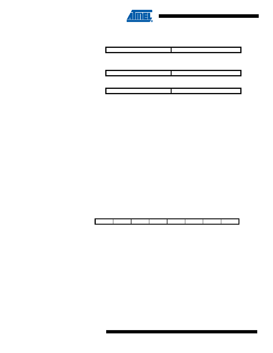
Figure 4-3.
The X-, Y-, and Z-registers
In the different addressing modes these address registers have functions as fixed displacement,
automatic increment, and automatic decrement (see the instruction set reference for details).
4.5
Stack Pointer
The Stack is mainly used for storing temporary data, for storing local variables and for storing
return addresses after interrupts and subroutine calls. The Stack Pointer Register always points
to the top of the Stack. Note that the Stack is implemented as growing from higher memory loca-
tions to lower memory locations. This implies that a Stack PUSH command decreases the Stack
Pointer.
The Stack Pointer points to the data SRAM Stack area where the Subroutine and Interrupt
Stacks are located. This Stack space in the data SRAM must be defined by the program before
any subroutine calls are executed or interrupts are enabled. The Stack Pointer must be set to
point above 0x60. The Stack Pointer is decremented by one when data is pushed onto the Stack
with the PUSH instruction, and it is decremented by two when the return address is pushed onto
the Stack with subroutine call or interrupt. The Stack Pointer is incremented by one when data is
popped from the Stack with the POP instruction, and it is incremented by two when data is
popped from the Stack with return from subroutine RET or return from interrupt RETI.
The Stack Pointer is implemented as one 8-bit register in the I/O space.
4.6
Instruction Execution Timing
This section describes the general access timing concepts for instruction execution. The AVR
CPU is driven by the CPU clock clk
CPU, directly generated from the selected clock source for the
chip. No internal clock division is used.
Figure 4-4 shows the parallel instruction fetches and instruction executions enabled by the Har-
vard architecture and the fast-access Register File concept. This is the basic pipelining concept
to obtain up to 1 MIPS per MHz with the corresponding unique results for functions per cost,
functions per clocks, and functions per power-unit.
15
XH
XL
0
X-register
70
7
0
R27 (0x1B)
R26 (0x1A)
15
YH
YL
0
Y-register
70
7
0
R29 (0x1D)
R28 (0x1C)
15
ZH
ZL
0
Z-register
70
7
0
R31 (0x1F)
R30 (0x1E)
Bit
7
65
43
21
0
SP7
SP6
SP5
SP4
SP3
SP2
SP1
SP0
SPL
Read/Write
R/W
Initial Value
RAMEND
相關PDF資料 |
PDF描述 |
|---|---|
| MQ80C52TXXX-20SB | 8-BIT, MROM, 20 MHz, MICROCONTROLLER, CQFP44 |
| IQ83C154DTXXX-L16D | 8-BIT, MROM, 16 MHz, MICROCONTROLLER, CQFP44 |
| IS80C32E-16SHXXX | 8-BIT, 16 MHz, MICROCONTROLLER, PQCC44 |
| IF283C154XXX-L16R | 8-BIT, MROM, 16 MHz, MICROCONTROLLER, PQFP44 |
| IF280C32-36SHXXX:R | 8-BIT, 36 MHz, MICROCONTROLLER, PQFP44 |
相關代理商/技術參數(shù) |
參數(shù)描述 |
|---|---|
| MD80C154-L16 | 制造商:TEMIC 制造商全稱:TEMIC Semiconductors 功能描述:CMOS 0 to 36 MHz Single Chip 8-bit Microcontroller |
| MD80C187-10/B | 制造商:Rochester Electronics LLC 功能描述: |
| MD80C187-12/B | 制造商:Rochester Electronics LLC 功能描述: |
| MD80C287-10/B | 制造商:Rochester Electronics LLC 功能描述: |
| MD80C31BH | 制造商:Rochester Electronics LLC 功能描述: |
發(fā)布緊急采購,3分鐘左右您將得到回復。