- 您現(xiàn)在的位置:買賣IC網(wǎng) > PDF目錄371096 > MCM72PB8ML4 (MOTOROLA INC) 256K x 72 Bit Burst RAM Multichip Module PDF資料下載
參數(shù)資料
| 型號: | MCM72PB8ML4 |
| 廠商: | MOTOROLA INC |
| 元件分類: | DRAM |
| 英文描述: | 256K x 72 Bit Burst RAM Multichip Module |
| 中文描述: | 256K X 72 CACHE SRAM MODULE, 4 ns, PBGA209 |
| 封裝: | PLASTIC, BGA-209 |
| 文件頁數(shù): | 5/20頁 |
| 文件大小: | 252K |
| 代理商: | MCM72PB8ML4 |
MCM72FB8ML MCM72PB8ML
5
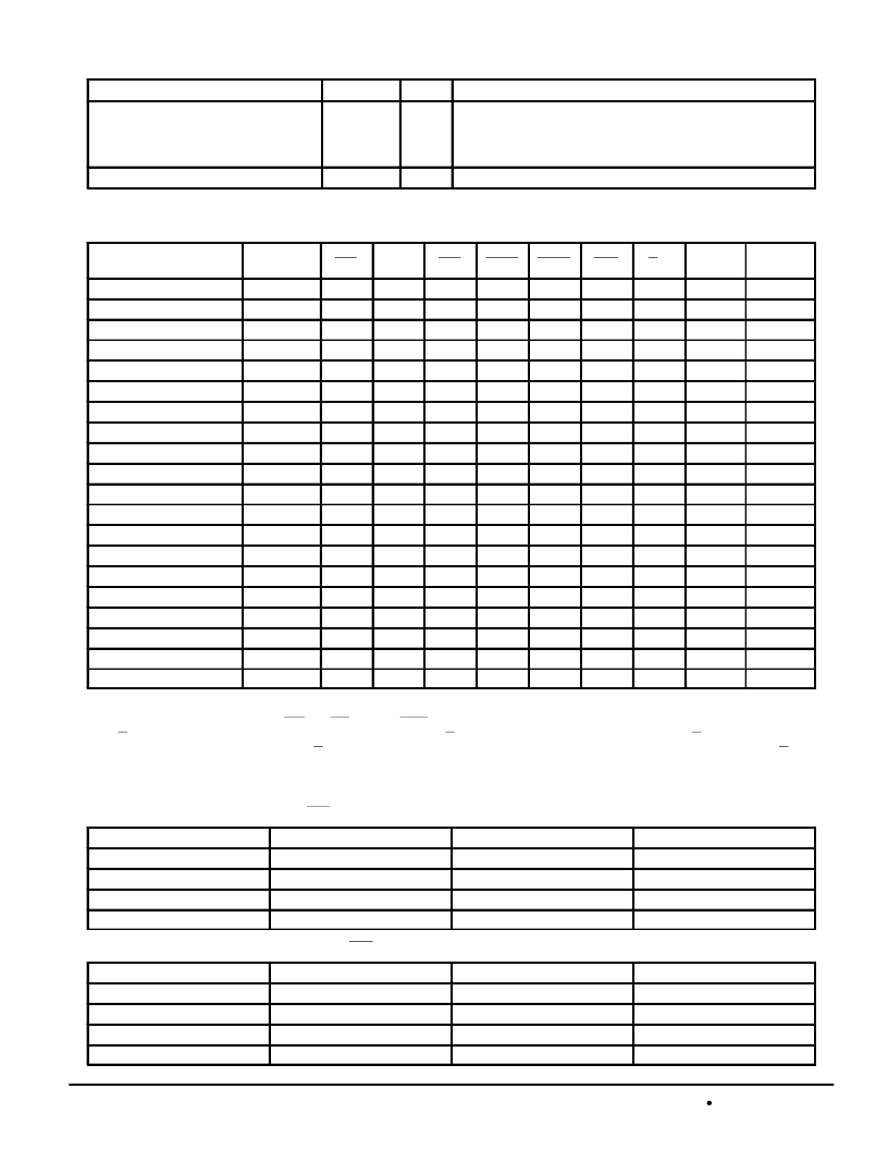
MOTOROLA FAST SRAM
PIN DESCRIPTIONS
(continued)
Pin Locations
Symbol
Type
Description
D9, D11, E9, E11, F9, F11, G9 – G11,
H8 – H12, J8 – J12, K8 – K12, L8 – L12,
M8 – M12, N9 – N11, P9, P11, R9, R11,
T9, T11
VSS
Supply
Ground.
K7, K13, P10, V7, V13, W7 – W13
NC
—
No Connection: There is no connection to the chip.
TRUTH TABLE
(See Notes 1 through 5)
Next Cycle
Address
Used
SE1
SE2
SE3
ADSP
ADSC
ADV
G 3
DQx
Write 2, 4
Deselect
None
1
X
X
X
0
X
X
High–Z
X
Deselect
None
0
X
1
0
X
X
X
High–Z
X
Deselect
None
0
0
X
0
X
X
X
High–Z
X
Deselect
None
X
X
1
1
0
X
X
High–Z
X
Deselect
None
X
0
X
1
0
X
X
High–Z
X
X5
Begin Read
External
0
1
0
0
X
X
X
High–Z
Begin Read
External
0
1
0
1
0
X
X
High–Z
READ5
Continue Read
Next
X
X
X
1
1
0
1
High–Z
READ
Continue Read
Next
X
X
X
1
1
0
0
DQ
READ
Continue Read
Next
1
X
X
X
1
0
1
High–Z
READ
Continue Read
Next
1
X
X
X
1
0
0
DQ
READ
Suspend Read
Current
X
X
X
1
1
1
1
High–Z
READ
Suspend Read
Current
X
X
X
1
1
1
0
DQ
READ
Suspend Read
Current
1
X
X
X
1
1
1
High–Z
READ
Suspend Read
Current
1
X
X
X
1
1
0
DQ
READ
Begin Write
External
0
1
0
1
0
X
X
High–Z
WRITE
Continue Write
Next
X
X
X
1
1
0
X
High–Z
WRITE
Continue Write
Next
1
X
X
X
1
0
X
High–Z
WRITE
Suspend Write
Current
X
X
X
1
1
1
X
High–Z
WRITE
Suspend Write
Current
1
X
X
X
1
1
X
High–Z
WRITE
NOTES:
1. X = Don’t Care. 1 = logic high. 0 = logic low.
2. Write is defined as either 1) any SBx and SW low or 2) SGW is low.
3. G is an asynchronous signal and is not sampled by the clock K. G drives the bus immediately (tGLQX) following G going low.
4. On write cycles that follow read cycles, G must be negated prior to the start of the write cycle to ensure proper write data setup times. G must
also remain negated at the completion of the write cycle to ensure proper write data hold times.
5. This read assumes the RAM was previously deselected.
LINEAR BURST ADDRESS TABLE
(LBO = VSS)
1st Address (External)
2nd Address (Internal)
3rd Address (Internal)
4th Address (Internal)
X . . . X00
X . . . X01
X . . . X10
X . . . X11
X . . . X01
X . . . X10
X . . . X11
X . . . X00
X . . . X10
X . . . X11
X . . . X00
X . . . X01
X . . . X11
X . . . X00
X . . . X01
X . . . X10
INTERLEAVED BURST ADDRESS TABLE
(LBO = VDD)
1st Address (External)
2nd Address (Internal)
3rd Address (Internal)
4th Address (Internal)
X . . . X00
X . . . X01
X . . . X10
X . . . X11
X . . . X01
X . . . X00
X . . . X11
X . . . X10
X . . . X10
X . . . X11
X . . . X00
X . . . X01
X . . . X11
X . . . X10
X . . . X01
X . . . X00
相關(guān)PDF資料 |
PDF描述 |
|---|---|
| MCM72PB8ML4R | 256K x 72 Bit Burst RAM Multichip Module |
| MCM72FB8ML7.5 | 256K x 72 Bit Burst RAM Multichip Module |
| MCM72FB8ML7.5R | CAP CER 680PF 100V C0G 0603 |
| MCM72FB8ML | 600000 SYSTEM GATE 1.8 VOLT FPGA - NOT RECOMMENDED for NEW DESIGN |
| MCM72FB8ML8 | 600,000 SYSTEM GATE 1.8 VOLT FPGA - NOT RECOMMENDED for NEW DESIGN |
相關(guān)代理商/技術(shù)參數(shù) |
參數(shù)描述 |
|---|---|
| MCM72PB8ML4R | 制造商:MOTOROLA 制造商全稱:Motorola, Inc 功能描述:256K x 72 Bit Burst RAM Multichip Module |
| MCM-7312 | 制造商:未知廠家 制造商全稱:未知廠家 功能描述:Four independent, RS-232-C, Full-duplex, Serial Communications Channels. |
| MCM-7314 | 制造商:未知廠家 制造商全稱:未知廠家 功能描述:Four independent, RS-232-C, Full-duplex, Serial Communications Channels. |
| MCM7643 | 制造商:MOTOROLA 制造商全稱:Motorola, Inc 功能描述:4096 BIT PROGRAMMABLE READ ONLY MEMORIES |
| MCM7643A | 制造商:MOTOROLA 制造商全稱:Motorola, Inc 功能描述:4096 BIT PROGRAMMABLE READ ONLY MEMORIES |
發(fā)布緊急采購,3分鐘左右您將得到回復(fù)。