- 您現(xiàn)在的位置:買賣IC網(wǎng) > PDF目錄371096 > MCM72F10 (Motorola, Inc.) 8MB Synchronous Fast Static RAM Module PDF資料下載
參數(shù)資料
| 型號(hào): | MCM72F10 |
| 廠商: | Motorola, Inc. |
| 英文描述: | 8MB Synchronous Fast Static RAM Module |
| 中文描述: | 8MB的同步快速靜態(tài)存儲(chǔ)器模塊 |
| 文件頁(yè)數(shù): | 8/12頁(yè) |
| 文件大小: | 167K |
| 代理商: | MCM72F10 |
MCM72F8
MCM72F9
8
MOTOROLA FAST SRAM
AC OPERATING CONDITIONS AND CHARACTERISTICS
(VDD = 3.3 V + 10%, – 5%, TA = 0 to 70
°
C, Unless Otherwise Noted)
Input Timing Measurement Reference Level
Input Pulse Levels
. . . . . . . . . . . . . . . . . . . . . . . . . . . . . . . . .
Input Rise/Fall Time
. . . . . . . . . . . . . . . . . . . . . . .
1.25 V
0 to 2.5 V
. . . . . . . . . . . . . .
1 V/ns (20 to 80%)
Output Timing Reference Level
Output Load
. . . . . . . . . . . . . .
1.25 V
. . . . . . . . . . . . . . . . . . . . . . . . .
See Figure 2 Unless Otherwise Noted
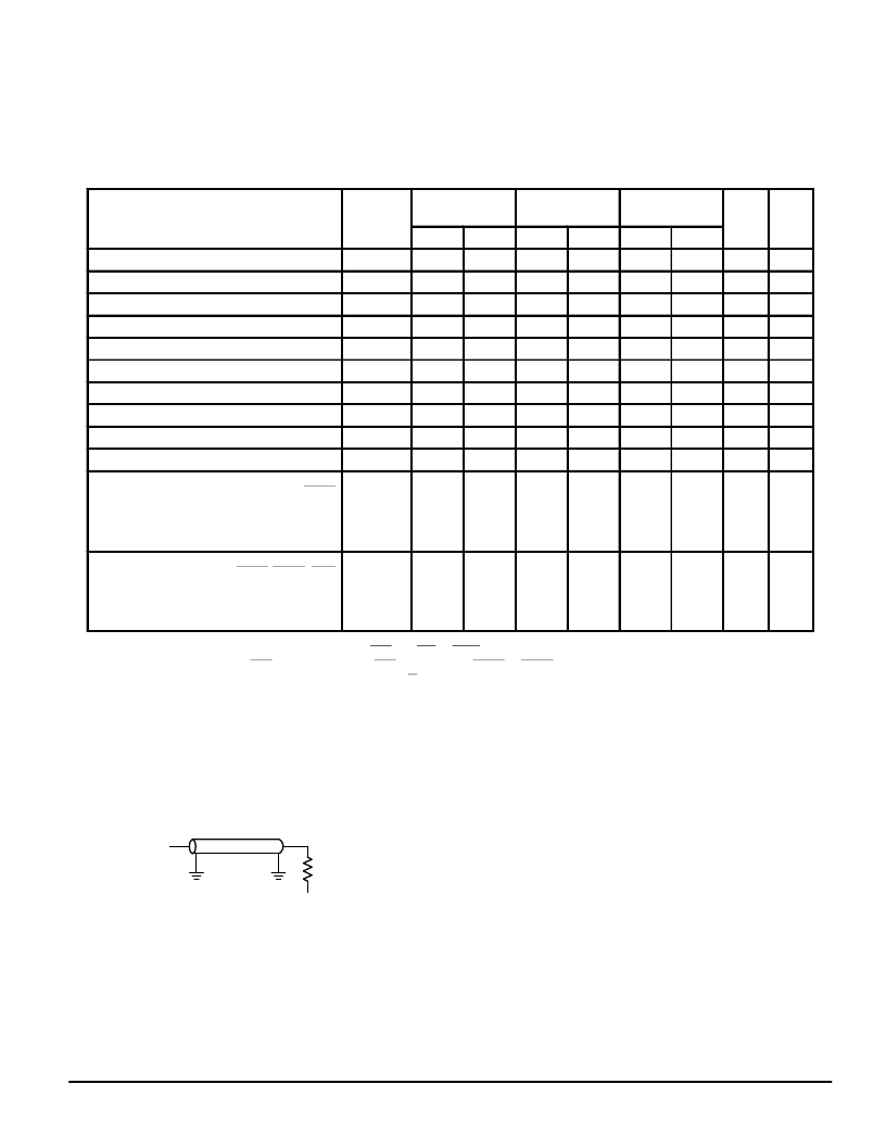
DATA RAMs READ/WRITE CYCLE TIMING
(See Notes 1, 2, and 3)
Parameter
Symbol
b l
MCM72F8–8
MCM72F9–8
MCM72F8–9
MCM72F9–9
MCM72F8–12
MCM72F9–12
U i
Unit
Notes
Min
Max
Min
Max
Min
Max
Cycle Time
tKHKH
tKHQV
tGLQV
tKHQX1
tKHQX2
tGLQX
tGHQZ
tKHQZ
tKHKL
tKLKH
tAVKH
tADKH
tDVKH
tWVKH
tEVKH
10
—
11
—
16.6
—
ns
Clock Access Time
—
8
—
9
—
12
ns
Output Enable to Output Valid
—
3.5
—
3.5
—
5
ns
Clock High to Output Active
0
—
0
—
0
—
ns
4, 5
Clock High to Output Change
2
—
2
—
2
—
ns
4
Output Enable to Output Active
0
—
0
—
0
—
ns
4, 5
Output Disable to Q High–Z
—
3.5
—
3.5
—
3.5
ns
4, 5
Clock High to Q High–Z
2
3.5
2
3.5
2
3.5
ns
4, 5
Clock High Pulse Width
4
—
4.5
—
5
—
ns
Clock Low Pulse Width
4
—
4.5
—
5
—
ns
Setup Times:
Address
ADSP
Data In
Write
Chip Enable
2
—
2
—
2
—
ns
Hold Times:
Address
ADSP, ADSC, ADV
Data In
Write
Chip Enable
tKHAX
tKHADX
tKHDX
tKHWX
tKHEX
0.5
—
0.5
—
0.5
—
ns
NOTES:
1. In setup and hold times, write refers to either any SBx and SW or SGW is low.
2. Chip enable is defined as SE1 low, SE2 high, and SE3 low whenever ADSP or ADSC is asserted.
3. All read and write cycle timings are referenced from K or G.
4. This parameter is sampled and not 100% tested.
5. Measured at
±
200 mV from steady state.
OUTPUT
Z0 = 50
RL = 50
VL = 1.25 V
TIMING LIMITS
The table of timing values shows either a minimum or a
maximum limit for each parameter. Input requirements are
specified from the external system point of view. Thus, ad-
dress setup time is shown as a minimum since the system
must supply at least that much time (even though most
devices do not require it). On the other hand, responses
from the memory are specified from the device point of
view. Thus, the access time is shown as a maximum since
the device never provides data later than that time.
Figure 2. AC Test Load
相關(guān)PDF資料 |
PDF描述 |
|---|---|
| MCM72BA32SG66 | 256KB and 512KB BurstRAM Secondary Cache Module for Pentium |
| MCM72BB32SG66 | 256KB and 512KB BurstRAM Secondary Cache Module for Pentium |
| MCM72BF32SG66 | 256KB and 512KB BurstRAM Secondary Cache Module for Pentium |
| MCM72CB32SG66 | 256KB and 512KB BurstRAM Secondary Cache Module for Pentium |
| MCM72BA64SG60 | 256KB and 512KB BurstRAM Secondary Cache Module for Pentium |
相關(guān)代理商/技術(shù)參數(shù) |
參數(shù)描述 |
|---|---|
| MCM72F10DG12 | 制造商:MOTOROLA 制造商全稱:Motorola, Inc 功能描述:8MB Synchronous Fast Static RAM Module |
| MCM72F10DG8 | 制造商:MOTOROLA 制造商全稱:Motorola, Inc 功能描述:8MB Synchronous Fast Static RAM Module |
| MCM72F10DG9 | 制造商:MOTOROLA 制造商全稱:Motorola, Inc 功能描述:8MB Synchronous Fast Static RAM Module |
| MCM72F6 | 制造商:MOTOROLA 制造商全稱:Motorola, Inc 功能描述:512KB and 1MB Synchronous Fast Static RAM Module |
| MCM72F6A | 制造商:MOTOROLA 制造商全稱:Motorola, Inc 功能描述:512KB and 1MB Synchronous Fast Static RAM Module |
發(fā)布緊急采購(gòu),3分鐘左右您將得到回復(fù)。