- 您現(xiàn)在的位置:買賣IC網(wǎng) > PDF目錄359643 > MCM63R836FC3.0R (飛思卡爾半導(dǎo)體(中國)有限公司) MCM63R836 PDF資料下載
參數(shù)資料
| 型號: | MCM63R836FC3.0R |
| 廠商: | 飛思卡爾半導(dǎo)體(中國)有限公司 |
| 英文描述: | MCM63R836 |
| 中文描述: | MCM63R836 |
| 文件頁數(shù): | 8/21頁 |
| 文件大小: | 363K |
| 代理商: | MCM63R836FC3.0R |
MCM63R836
MCM63R918
8
MOTOROLA FAST SRAM
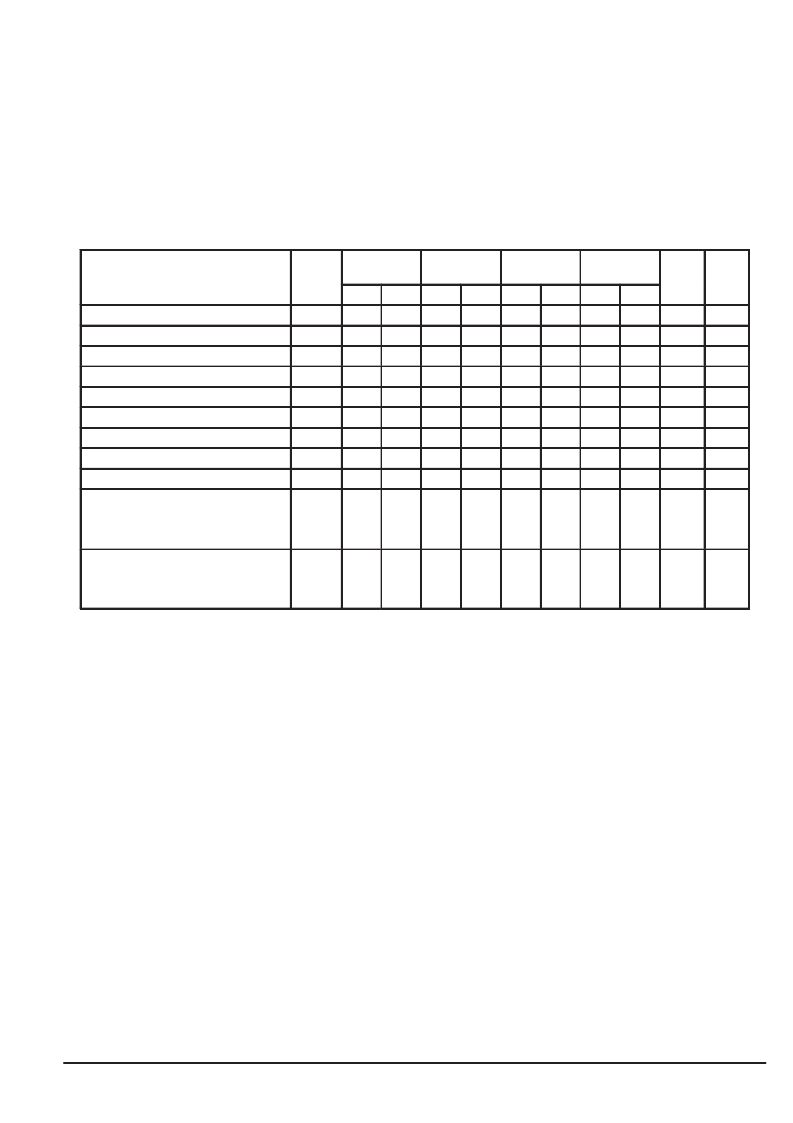
AC OPERATING CONDITIONS AND CHARACTERISTICS
(2.375 V
≤
VDD
≤
3.6 V, 0
°
C
≤
TA
≤
70
°
C, Unless Otherwise Noted)
Input Pulse Levels
Input Rise/Fall Time
Input Timing Measurement Reference Level
Output Timing Reference Level
0.25 to 1.25 V
1 V/ns (20% to 80%)
. . . . . . . . . . . . . .
. . . . . . . . . . . . . . . . . . . . . . . . . . . . . .
. . . . . . . . . . . . . . . . . . . . . .
0.75 V
0.75 V
. . . . . . . . . . . . . . . . . . . . . . . . .
Clock Input Timing Reference Level
ZQ for 50
Impedance
R
θ
JA Device
. . . . . . . . . . . . . . . . . . . . . . . . . . . . . . . . . . . . . . . .
Differential Cross–Point
. . . . . .
250
22 C/W
. . . . . . . . . . . . . . . . . . . . . . . . . . . . . . . .
READ/WRITE CYCLE TIMING
(See Note 1)
63R836–3.0
63R918–3.0
63R836–3.3
63R918–3.3
63R836–3.7
63R918–3.7
63R836–4.0
63R918–4.0
Parameter
Symbol
Min
Max
Min
Max
Min
Max
Min
Max
Unit
Notes
Cycle Time
tKHKH
tKHKL
tKLKH
tKHQX1
tKHQV
tKHQX
tKHQZ
tZZE
tZZR
tAVKH
tDVKH
tSVKH
tWVKH
tKHAX
tKHDX
tKHSX
tKHWX
3
—
3.3
—
3.7
—
4
—
ns
Clock High Pulse Width
1.2
—
1.2
—
1.5
—
1.5
—
ns
Clock Low Pulse Width
1.2
—
1.2
—
1.5
—
1.5
—
ns
Clock High to Output Low–Z
0.5
—
0.5
—
0.5
—
0.5
—
ns
1, 2
Clock High to Output Valid
—
1.5
—
1.65
—
1.85
—
2
ns
Clock High to Output Hold
0.5
—
0.5
—
0.5
—
0.5
—
ns
1
Clock High to Output High–Z
—
1.5
—
1.6
—
1.7
—
2
ns
1, 3
ZZ High to Sleep Mode
3
—
3.3
—
3.7
—
4
—
ns
ZZ Low to Recovery
—
10
—
10
—
10
—
10
ns
Setup Times:
Address
Data In
Chip Select
Write Enable
0.5
—
0.5
—
0.5
—
0.5
—
ns
Hold Times:
Address
Data In
Chip Select
Write Enable
0.5
—
0.5
—
0.5
—
0.5
—
ns
NOTES:
1. This parameter is sampled and not 100% tested.
2. Measured at
±
200 mV from steady state.
3. Measured at
±
200 mV from steady state. See Test Load Figure 1b.
F
Freescale Semiconductor, Inc.
For More Information On This Product,
Go to: www.freescale.com
n
.
相關(guān)PDF資料 |
PDF描述 |
|---|---|
| MCM63R836FC3.3 | MCM63R836 |
| MCM63R836FC3.3R | MCM63R836 |
| MCM63R836FC3.7 | MCM63R836 |
| MCM63R836FC3.7R | MCM63R836 |
| MCM63R836FC4.0 | MCM63R836 |
相關(guān)代理商/技術(shù)參數(shù) |
參數(shù)描述 |
|---|---|
| MCM63R836FC4.0 | 制造商:FREESCALE 制造商全稱:Freescale Semiconductor, Inc 功能描述:MCM63R836 |
| MCM63R836FC4.0R | 制造商:FREESCALE 制造商全稱:Freescale Semiconductor, Inc 功能描述:MCM63R836 |
| MCM63R918 | 制造商:FREESCALE 制造商全稱:Freescale Semiconductor, Inc 功能描述:MCM63R836 |
| MCM63R918FC3.0 | 制造商:FREESCALE 制造商全稱:Freescale Semiconductor, Inc 功能描述:MCM63R836 |
| MCM63R918FC3.0R | 制造商:FREESCALE 制造商全稱:Freescale Semiconductor, Inc 功能描述:MCM63R836 |
發(fā)布緊急采購,3分鐘左右您將得到回復(fù)。