- 您現(xiàn)在的位置:買賣IC網(wǎng) > PDF目錄371083 > MCM62110FN20 (MOTOROLA INC) 32K x 9 Bit Synchronous Dual I/O or Separate I/O Fast Static RAM with Parity Checker PDF資料下載
參數(shù)資料
| 型號(hào): | MCM62110FN20 |
| 廠商: | MOTOROLA INC |
| 元件分類: | SRAM |
| 英文描述: | 32K x 9 Bit Synchronous Dual I/O or Separate I/O Fast Static RAM with Parity Checker |
| 中文描述: | 32K X 9 APPLICATION SPECIFIC SRAM, PQCC52 |
| 封裝: | PLASTIC, LCC-52 |
| 文件頁(yè)數(shù): | 7/12頁(yè) |
| 文件大?。?/td> | 206K |
| 代理商: | MCM62110FN20 |
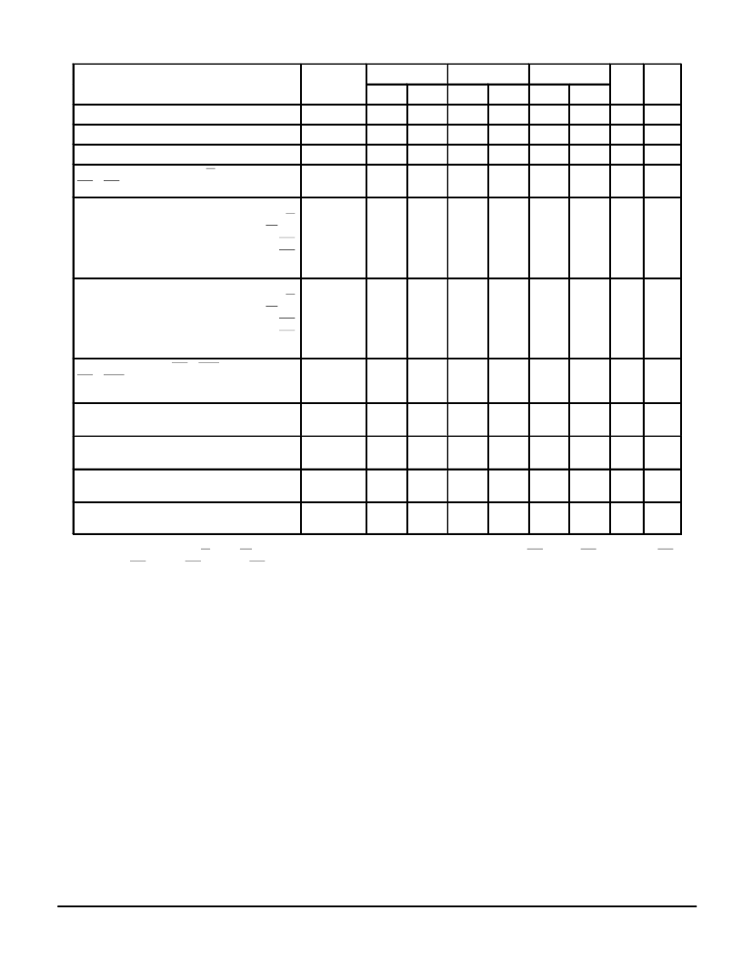
MCM62110
7
MOTOROLA FAST SRAM
WRITE CYCLE
(See Note 1)
MCM62110–15
MCM62110–17
MCM62110–20
Parameter
Symbol
Min
Max
Min
Max
Min
Max
Unit
Notes
Write Cycle Times
tKHKH
15
—
17
—
20
—
ns
1, 2
Clock Low Pulse Width
tKLKH
5
—
5
—
5
—
ns
Clock High Pulse Width
tKHKL
7
—
7
—
7
—
ns
Clock High to Output High–Z (W = VIL and
SIE = PIE = VIH)
tKHQZ
—
8
—
9
—
10
ns
3, 4
Setup Times:
A
W
E1, E2
PIE
SIE
SDQ0 – SDQ7, SDQP, PDQ0 – PDQ7, PDQP
tAVKL
tWLKH
tEVKL
tPIEVKH
tSIEVKH
tDVKH
2.5
—
2.5
—
2.5
—
ns
Hold Times:
A
W
E1, E2
PIE
SIE
SDQ0 – SDQ7, SDQP, PDQ0 – PDQ7, PDQP
tKLAX
tKHWX
tKLEX
tKHPIEX
tKHSIEX
tKHDX
2
—
2
—
2
—
ns
Write with Streaming (PIE = SOE = VIL or
SIE = POE = VIL)
Clock High to Output Valid
tKHQV
—
7
—
7.5
—
8
ns
5
Output Enable High to Q High–Z
tPOEHQZ
tSOEHQZ
0
8
0
9
0
9
ns
6
Output Hold from Output Enable High
tPOEHQX
tSOEHQX
5
—
5
—
5
—
ns
Output Enable Low to Q Active
tPOELQX
tSOELQX
0
—
0
—
0
—
ns
6
Output Enable Low to Output Valid
tPOELQV
tSOELQV
—
5
—
6
—
8
ns
NOTES:
1. A write is performed with W = VIL, E1 = VIL, E2 = VIH for the specified setup and hold times and either PIE = VIL or SIE = VIL. If both PIE =
VIL and SIE = VIL or PIE = VIH and SIE = VIH, then this is treated like a NOP and no write is performed.
2. All write cycle timings are referenced from K.
3. K must be at a high level for the outputs to transition.
4. Transition is measured
±
500 mV from steady–state voltage with output load of Figure 1B. This parameter is sampled and not 100% tested.
At any given voltage and temperature, tKHQZ is less than tKHQX for a given device.
5. A write with streaming is defined as a write cycle which writes data from one data bus to the array and outputs the same data onto the other
data bus.
6. Transition is measured
±
500 mV from steady–state voltage with output load of Figure 1B. This parameter is sampled and not 100% tested.
At any given voltage and temperature, tKHQZ is less than tKHQX, tPOEHQZ is less than tPOELQX for a given device, and tSOEHQZ is less
than tSOELQX for a given device.
相關(guān)PDF資料 |
PDF描述 |
|---|---|
| MCM6226BB | 128K x 8 Bit Static Random Access Memory |
| MCM6226BBXJ35R2 | 128K x 8 Bit Static Random Access Memory |
| MCM6226BBXJ20 | 128K x 8 Bit Static Random Access Memory |
| MCM6226BBXJ20R2 | 128K x 8 Bit Static Random Access Memory |
| MCM6226BBXJ25 | 128K x 8 Bit Static Random Access Memory |
相關(guān)代理商/技術(shù)參數(shù) |
參數(shù)描述 |
|---|---|
| MCM6223YJ15 | 制造商:Motorola Inc 功能描述: |
| MCM6226BAXJ20 | 制造商:Motorola Inc 功能描述: |
| MCM6226BB | 制造商:MOTOROLA 制造商全稱:Motorola, Inc 功能描述:128K x 8 Bit Static Random Access Memory |
| MCM6226BBEJ15 | 制造商:Motorola Inc 功能描述: |
| MCM6226BBEJ15R2 | 制造商:MOTOROLA 制造商全稱:Motorola, Inc 功能描述:128K x 8 Bit Static Random Access Memory |
發(fā)布緊急采購(gòu),3分鐘左右您將得到回復(fù)。