- 您現(xiàn)在的位置:買賣IC網(wǎng) > PDF目錄371081 > MCM56824AZP20 (MOTOROLA INC) 8K x 24 Bit Fast Static RAM PDF資料下載
參數(shù)資料
| 型號: | MCM56824AZP20 |
| 廠商: | MOTOROLA INC |
| 元件分類: | DRAM |
| 英文描述: | 8K x 24 Bit Fast Static RAM |
| 中文描述: | 8K X 24 APPLICATION SPECIFIC SRAM, 20 ns, PBGA86 |
| 封裝: | PLASTIC, BGA-86 |
| 文件頁數(shù): | 5/10頁 |
| 文件大小: | 147K |
| 代理商: | MCM56824AZP20 |
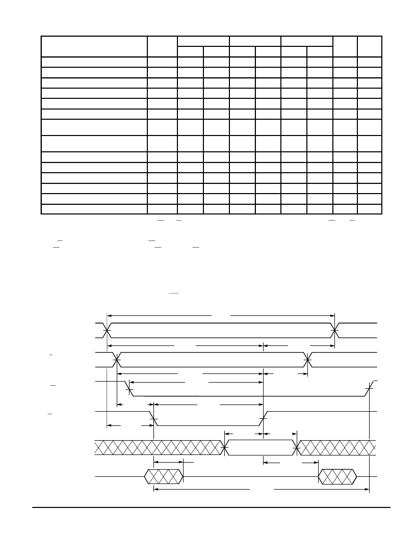
MCM56824A
5
MOTOROLA FAST SRAM
WRITE CYCLE TIMING
(Write Enable Initiated, See Note 1)
MCM56824A–20
MCM56824A–25
MCM56824A–35
Parameter
Symbol
Min
Max
Min
Max
Min
Max
Unit
Notes
Write Cycle Time
tAVAV
tAVWL
tVSVWL
tAVWH
tVSVWH
tWLWH
tWLE1H
tWLE2L
tE1LWH
tE2HWH
tDVWH
tWHDX
tWHAX
tWHVSX
tWHQX
tWLQZ
20
—
25
—
35
—
ns
Address Setup Time
0
—
0
—
0
—
ns
2
MUX Control Setup Time
0
—
0
—
0
—
ns
Address Valid to End of Write
15
—
20
—
30
—
ns
MUX Control Valid to End of Write
15
—
20
—
30
—
ns
Write Pulse Width
15
—
15
—
20
—
ns
3
Write Enable to Chip Enable Disable
15
—
15
—
20
—
ns
3, 4
Chip Enable to End of Write
15
—
15
—
20
—
ns
3, 4
Data Valid to End of Write
8
—
10
—
15
—
ns
Data Hold Time
0
—
0
—
0
—
ns
5
Write Recovery Time
0
—
0
—
0
—
ns
2
MUX Control Recovery Time
0
—
0
—
0
—
ns
Write High to Output Low–Z
4
—
5
—
5
—
ns
6
Write Low to Output High–Z
0
15
0
15
0
15
ns
6
NOTES:
1. A write cycle starts at the latest transition of E1 low, W low, or E2 high. A write cycle ends at the earliest transition of E1 high, W high, or E2
low.
2. Write must be high for all address transitions.
3. If W goes low coincident with or prior to E1 low or E2 high the outputs will remain in a high–impedance state.
4. E1 in the timing diagrams represents both E1 and E2 with E1 asserted low and E2 asserted high.
5. During this time the output pins may be in the output state. Signals of opposite phase must not be applied to the outputs at this time.
6. Transition is measured
±
500 mV from steady–state voltage with load of Figure 1b. This parameter is sampled and not 100% tested. At any
given voltage and temperature, tE1HQZ max is less than tE1LQX min, tE2LQZ max is less than tE2HQX min, and tGHQZ max is less than
tGLQX min for a given device and from device to device.
WE INITIATED WRITE CYCLE
HIGH–Z
HIGH–Z
E1 (CHIP ENABLE)
VALID DATA IN
D (DATA IN)
W (WRITE ENABLE)
V/S (MUX CONTROL)
Q (DATA OUT)
A (ADDRESS)
tAVAV
tWHQX
tDVWH
tWLQZ
tWHAX
tWHDX
tWHVSX
tAVWL
tE1LWH
tVSVWL
tWLWH
tVSVWH
tAVWH
tWLE1H
相關(guān)PDF資料 |
PDF描述 |
|---|---|
| MCM56824AZP20R2 | 8K x 24 Bit Fast Static RAM |
| MCM56824AZP25R2 | ER 35C 28#16 7#12 SKT PLUG |
| MCM56824AZP35 | 8K x 24 Bit Fast Static RAM |
| MCM56824AZP35R2 | 8K x 24 Bit Fast Static RAM |
| MCM56824A | 8K x 24 Bit Fast Static RAM |
相關(guān)代理商/技術(shù)參數(shù) |
參數(shù)描述 |
|---|---|
| MCM56824AZP20R2 | 制造商:MOTOROLA 制造商全稱:Motorola, Inc 功能描述:8K x 24 Bit Fast Static RAM |
| MCM56824AZP25R2 | 制造商:MOTOROLA 制造商全稱:Motorola, Inc 功能描述:8K x 24 Bit Fast Static RAM |
| MCM56824AZP35 | 制造商:MOTOROLA 制造商全稱:Motorola, Inc 功能描述:8K x 24 Bit Fast Static RAM |
| MCM56824AZP35R2 | 制造商:MOTOROLA 制造商全稱:Motorola, Inc 功能描述:8K x 24 Bit Fast Static RAM |
| MCM60256AP10 | 制造商: 功能描述: 制造商:undefined 功能描述: |
發(fā)布緊急采購,3分鐘左右您將得到回復(fù)。