- 您現(xiàn)在的位置:買賣IC網(wǎng) > PDF目錄45313 > MCIMX31CVKN5CR2 (FREESCALE SEMICONDUCTOR INC) 532 MHz, MICROPROCESSOR, PBGA457 PDF資料下載
參數(shù)資料
| 型號: | MCIMX31CVKN5CR2 |
| 廠商: | FREESCALE SEMICONDUCTOR INC |
| 元件分類: | 微控制器/微處理器 |
| 英文描述: | 532 MHz, MICROPROCESSOR, PBGA457 |
| 封裝: | 14 X 14 MM, 0.50 MM PITCH, ROHS COMPLIANT, MAPBGA-457 |
| 文件頁數(shù): | 85/122頁 |
| 文件大小: | 1418K |
| 代理商: | MCIMX31CVKN5CR2 |
第1頁第2頁第3頁第4頁第5頁第6頁第7頁第8頁第9頁第10頁第11頁第12頁第13頁第14頁第15頁第16頁第17頁第18頁第19頁第20頁第21頁第22頁第23頁第24頁第25頁第26頁第27頁第28頁第29頁第30頁第31頁第32頁第33頁第34頁第35頁第36頁第37頁第38頁第39頁第40頁第41頁第42頁第43頁第44頁第45頁第46頁第47頁第48頁第49頁第50頁第51頁第52頁第53頁第54頁第55頁第56頁第57頁第58頁第59頁第60頁第61頁第62頁第63頁第64頁第65頁第66頁第67頁第68頁第69頁第70頁第71頁第72頁第73頁第74頁第75頁第76頁第77頁第78頁第79頁第80頁第81頁第82頁第83頁第84頁當前第85頁第86頁第87頁第88頁第89頁第90頁第91頁第92頁第93頁第94頁第95頁第96頁第97頁第98頁第99頁第100頁第101頁第102頁第103頁第104頁第105頁第106頁第107頁第108頁第109頁第110頁第111頁第112頁第113頁第114頁第115頁第116頁第117頁第118頁第119頁第120頁第121頁第122頁
Electrical Characteristics
MCIMX31/MCIMX31L Technical Data, Rev. 4.1
Freescale Semiconductor
65
4.3.15.4
Synchronous Interface to Dual-Port Smart Displays
Functionality and electrical characteristics of the synchronous interface to dual-port smart displays are
identical to parameters of the synchronous interface. See Section 4.3.15.2.2, “Interface to Active Matrix
4.3.15.4.1
Interface to a TV Encoder, Functional Description
The interface has an 8-bit data bus, transferring a single 8-bit value (Y/U/V) in each cycle. The bits
D7–D0 of the value are mapped to bits LD17–LD10 of the data bus, respectively. Figure 51 depicts the
interface timing,
The frequency of the clock DISPB_D3_CLK is 27 MHz (within 10%).
The DISPB_D3_HSYNC, DISPB_D3_VSYNC and DISPB_D3_DRDY signals are active low.
The transition to the next row is marked by the negative edge of the DISPB_D3_HSYNC signal. It
remains low for a single clock cycle.
The transition to the next field/frame is marked by the negative edge of the DISPB_D3_VSYNC
signal. It remains low for at least one clock cycle.
— At a transition to an odd field (of the next frame), the negative edges of DISPB_D3_VSYNC
and DISPB_D3_HSYNC coincide.
— At a transition to an even field (of the same frame), they do not coincide.
The active intervals—during which data is transferred—are marked by the DISPB_D3_HSYNC
signal being high.
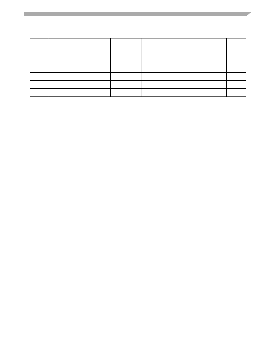
Table 49. Sharp Synchronous Display Interface Timing Parameters—Pixel Level
ID
Parameter
Symbol
Value
Units
IP21
SPL rise time
Tsplr
(BGXP – 1) * Tdpcp
ns
IP22
CLS rise time
Tclsr
CLS_RISE_DELAY * Tdpcp
ns
IP23
CLS fall time
Tclsf
CLS_FALL_DELAY * Tdpcp
ns
IP24
CLS rise and PS fall time
Tpsf
PS_FALL_DELAY * Tdpcp
ns
IP25
PS rise time
Tpsr
PS_RISE_DELAY * Tdpcp
ns
IP26
REV toggle time
Trev
REV_TOGGLE_DELAY * Tdpcp
ns
Because
of
an
order
from
the
United
States
International
Trade
Commission,
BGA-packaged
product
lines
and
part
numbers
indicated
here
currently
are
not
available
from
Freescale
for
import
or
sale
in
the
United
States
prior
to
September
2010:
i.MX31
Product
Family
相關(guān)PDF資料 |
PDF描述 |
|---|---|
| MCIMX31VKN5B | 532 MHz, MICROPROCESSOR, PBGA457 |
| MCIMX31LVKN5BR2 | 532 MHz, MICROPROCESSOR, PBGA457 |
| MCIMX31LVMN5C | 532 MHz, MICROPROCESSOR, PBGA473 |
| MCIMX31VKN5 | 532 MHz, MICROPROCESSOR, PBGA457 |
| MCIMX507CVM8B | SPECIALTY MICROPROCESSOR CIRCUIT, PBGA400 |
相關(guān)代理商/技術(shù)參數(shù) |
參數(shù)描述 |
|---|---|
| MCIMX31CVKN5D | 功能描述:處理器 - 專門應(yīng)用 2.0.1 CONSUMER FULL RoHS:否 制造商:Freescale Semiconductor 類型:Multimedia Applications 核心:ARM Cortex A9 處理器系列:i.MX6 數(shù)據(jù)總線寬度:32 bit 最大時鐘頻率:1 GHz 指令/數(shù)據(jù)緩存: 數(shù)據(jù) RAM 大小:128 KB 數(shù)據(jù) ROM 大小: 工作電源電壓: 最大工作溫度:+ 95 C 安裝風格:SMD/SMT 封裝 / 箱體:MAPBGA-432 |
| MCIMX31CVKN5DR2 | 功能描述:處理器 - 專門應(yīng)用 2.0.1 CONSUMER FULL RoHS:否 制造商:Freescale Semiconductor 類型:Multimedia Applications 核心:ARM Cortex A9 處理器系列:i.MX6 數(shù)據(jù)總線寬度:32 bit 最大時鐘頻率:1 GHz 指令/數(shù)據(jù)緩存: 數(shù)據(jù) RAM 大小:128 KB 數(shù)據(jù) ROM 大小: 工作電源電壓: 最大工作溫度:+ 95 C 安裝風格:SMD/SMT 封裝 / 箱體:MAPBGA-432 |
| MCIMX31CVMN4C | 功能描述:處理器 - 專門應(yīng)用 TORTOLA MX31 AUTO FULL RoHS:否 制造商:Freescale Semiconductor 類型:Multimedia Applications 核心:ARM Cortex A9 處理器系列:i.MX6 數(shù)據(jù)總線寬度:32 bit 最大時鐘頻率:1 GHz 指令/數(shù)據(jù)緩存: 數(shù)據(jù) RAM 大小:128 KB 數(shù)據(jù) ROM 大小: 工作電源電壓: 最大工作溫度:+ 95 C 安裝風格:SMD/SMT 封裝 / 箱體:MAPBGA-432 |
| MCIMX31CVMN4CR2 | 功能描述:處理器 - 專門應(yīng)用 TORTOLA MX31 AUTO FULL RoHS:否 制造商:Freescale Semiconductor 類型:Multimedia Applications 核心:ARM Cortex A9 處理器系列:i.MX6 數(shù)據(jù)總線寬度:32 bit 最大時鐘頻率:1 GHz 指令/數(shù)據(jù)緩存: 數(shù)據(jù) RAM 大小:128 KB 數(shù)據(jù) ROM 大小: 工作電源電壓: 最大工作溫度:+ 95 C 安裝風格:SMD/SMT 封裝 / 箱體:MAPBGA-432 |
| MCIMX31CVMN4D | 功能描述:處理器 - 專門應(yīng)用 2.0.1 AUTO FULL RoHS:否 制造商:Freescale Semiconductor 類型:Multimedia Applications 核心:ARM Cortex A9 處理器系列:i.MX6 數(shù)據(jù)總線寬度:32 bit 最大時鐘頻率:1 GHz 指令/數(shù)據(jù)緩存: 數(shù)據(jù) RAM 大小:128 KB 數(shù)據(jù) ROM 大小: 工作電源電壓: 最大工作溫度:+ 95 C 安裝風格:SMD/SMT 封裝 / 箱體:MAPBGA-432 |
發(fā)布緊急采購,3分鐘左右您將得到回復(fù)。