- 您現(xiàn)在的位置:買賣IC網(wǎng) > PDF目錄25625 > MC9S12C64MPBR2 (FREESCALE SEMICONDUCTOR INC) 16-BIT, FLASH, 25 MHz, MICROCONTROLLER, PQFP52 PDF資料下載
參數(shù)資料
| 型號: | MC9S12C64MPBR2 |
| 廠商: | FREESCALE SEMICONDUCTOR INC |
| 元件分類: | 微控制器/微處理器 |
| 英文描述: | 16-BIT, FLASH, 25 MHz, MICROCONTROLLER, PQFP52 |
| 封裝: | PLASTIC, LQFP-52 |
| 文件頁數(shù): | 365/680頁 |
| 文件大小: | 3497K |
| 代理商: | MC9S12C64MPBR2 |
Chapter 14 Serial Peripheral Interface (SPIV3) Block Description
Freescale Semiconductor
MC9S12C-Family / MC9S12GC-Family
427
Rev 01.23
Data reception is double buffered. Data is shifted serially into the SPI shift register during the transfer and
is transferred to the parallel SPI Data Register after the last bit is shifted in.
After the 16th (last) SCK edge:
Data that was previously in the master SPI Data Register should now be in the slave data register
and the data that was in the slave data register should be in the master.
The SPIF ag in the SPI Status Register is set indicating that the transfer is complete.
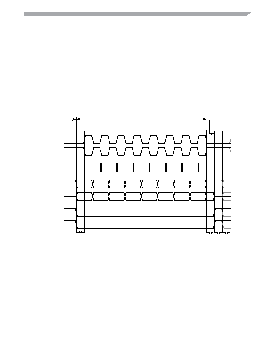
Figure 14-9 is a timing diagram of an SPI transfer where CPHA = 0. SCK waveforms are shown for
CPOL = 0 and CPOL = 1. The diagram may be interpreted as a master or slave timing diagram because
the SCK, MISO, and MOSI pins are connected directly between the master and the slave. The MISO signal
is the output from the slave and the MOSI signal is the output from the master. The SS pin of the master
must be either high or recongured as a general-purpose output not affecting the SPI.
Figure 14-9. SPI Clock Format 0 (CPHA = 0)
In slave mode, if the SS line is not deasserted between the successive transmissions then the content of the
SPI Data Register is not transmitted, instead the last received byte is transmitted. If the SS line is deasserted
for at least minimum idle time (half SCK cycle) between successive transmissions then the content of the
SPI Data Register is transmitted.
tL
Begin
End
SCK (CPOL = 0)
SAMPLE I
CHANGE O
SEL SS (O)
Transfer
SCK (CPOL = 1)
MSB rst (LSBFE = 0):
LSB rst (LSBFE = 1):
MSB
LSB
MSB
Bit 5
Bit 2
Bit 6
Bit 1
Bit 4
Bit 3
Bit 4
Bit 2
Bit 5
Bit 1
Bit 6
CHANGE O
SEL SS (I)
MOSI pin
MISO pin
Master only
MOSI/MISO
tT
If
ne
xt
tr
ansf
er
begins
here
for tT, tl, tL
Minimum 1/2 SCK
tI
tL
tL = Minimum leading time before the rst SCK edge
tT = Minimum trailing time after the last SCK edge
tI = Minimum idling time between transfers (minimum SS high time)
tL, tT, and tI are guaranteed for the master mode and required for the slave mode.
1
2
34
56
78
9
10
11
12
13 14
15
16
SCK Edge Nr.
End of Idle State
Begin of Idle State
相關(guān)PDF資料 |
PDF描述 |
|---|---|
| MC9S12C32CPB16 | 16-BIT, FLASH, 16 MHz, MICROCONTROLLER, PQFP52 |
| MC9S12C128MFA | 16-BIT, FLASH, 25 MHz, MICROCONTROLLER, PQFP48 |
| MC9S12C128CFUE | 16-BIT, FLASH, 25 MHz, MICROCONTROLLER, PQFP80 |
| MC9S12C128MPBER | 16-BIT, FLASH, 25 MHz, MICROCONTROLLER, PQFP52 |
| MC9S12GC16CFA | 16-BIT, FLASH, 25 MHz, MICROCONTROLLER, PQFP48 |
相關(guān)代理商/技術(shù)參數(shù) |
參數(shù)描述 |
|---|---|
| MC9S12C64VFAE | 功能描述:16位微控制器 - MCU 9S12C64 (KOI) RoHS:否 制造商:Texas Instruments 核心:RISC 處理器系列:MSP430FR572x 數(shù)據(jù)總線寬度:16 bit 最大時鐘頻率:24 MHz 程序存儲器大小:8 KB 數(shù)據(jù) RAM 大小:1 KB 片上 ADC:Yes 工作電源電壓:2 V to 3.6 V 工作溫度范圍:- 40 C to + 85 C 封裝 / 箱體:VQFN-40 安裝風(fēng)格:SMD/SMT |
| MC9S12C64VFUE | 功能描述:16位微控制器 - MCU 9S12C64 (KOI) RoHS:否 制造商:Texas Instruments 核心:RISC 處理器系列:MSP430FR572x 數(shù)據(jù)總線寬度:16 bit 最大時鐘頻率:24 MHz 程序存儲器大小:8 KB 數(shù)據(jù) RAM 大小:1 KB 片上 ADC:Yes 工作電源電壓:2 V to 3.6 V 工作溫度范圍:- 40 C to + 85 C 封裝 / 箱體:VQFN-40 安裝風(fēng)格:SMD/SMT |
| MC9S12C96CFAE | 功能描述:16位微控制器 - MCU 9S12C96-KOI-EPP RoHS:否 制造商:Texas Instruments 核心:RISC 處理器系列:MSP430FR572x 數(shù)據(jù)總線寬度:16 bit 最大時鐘頻率:24 MHz 程序存儲器大小:8 KB 數(shù)據(jù) RAM 大小:1 KB 片上 ADC:Yes 工作電源電壓:2 V to 3.6 V 工作溫度范圍:- 40 C to + 85 C 封裝 / 箱體:VQFN-40 安裝風(fēng)格:SMD/SMT |
| MC9S12C96CFU | 制造商:Freescale Semiconductor 功能描述:16-BIT, FLASH, 25 MHz, MICROCONTROLLER, PQFP80 |
| MC9S12C96CFUE | 功能描述:16位微控制器 - MCU 9S12C96 (KOI) - PB FREE RoHS:否 制造商:Texas Instruments 核心:RISC 處理器系列:MSP430FR572x 數(shù)據(jù)總線寬度:16 bit 最大時鐘頻率:24 MHz 程序存儲器大小:8 KB 數(shù)據(jù) RAM 大小:1 KB 片上 ADC:Yes 工作電源電壓:2 V to 3.6 V 工作溫度范圍:- 40 C to + 85 C 封裝 / 箱體:VQFN-40 安裝風(fēng)格:SMD/SMT |
發(fā)布緊急采購,3分鐘左右您將得到回復(fù)。