- 您現(xiàn)在的位置:買賣IC網(wǎng) > PDF目錄45292 > MC9S08SG4MTGR (FREESCALE SEMICONDUCTOR INC) 8-BIT, FLASH, 40 MHz, MICROCONTROLLER, PDSO16 PDF資料下載
參數(shù)資料
| 型號(hào): | MC9S08SG4MTGR |
| 廠商: | FREESCALE SEMICONDUCTOR INC |
| 元件分類: | 微控制器/微處理器 |
| 英文描述: | 8-BIT, FLASH, 40 MHz, MICROCONTROLLER, PDSO16 |
| 封裝: | ROHS COMPLIANT, TSSOP-16 |
| 文件頁數(shù): | 237/316頁 |
| 文件大小: | 3118K |
| 代理商: | MC9S08SG4MTGR |
第1頁第2頁第3頁第4頁第5頁第6頁第7頁第8頁第9頁第10頁第11頁第12頁第13頁第14頁第15頁第16頁第17頁第18頁第19頁第20頁第21頁第22頁第23頁第24頁第25頁第26頁第27頁第28頁第29頁第30頁第31頁第32頁第33頁第34頁第35頁第36頁第37頁第38頁第39頁第40頁第41頁第42頁第43頁第44頁第45頁第46頁第47頁第48頁第49頁第50頁第51頁第52頁第53頁第54頁第55頁第56頁第57頁第58頁第59頁第60頁第61頁第62頁第63頁第64頁第65頁第66頁第67頁第68頁第69頁第70頁第71頁第72頁第73頁第74頁第75頁第76頁第77頁第78頁第79頁第80頁第81頁第82頁第83頁第84頁第85頁第86頁第87頁第88頁第89頁第90頁第91頁第92頁第93頁第94頁第95頁第96頁第97頁第98頁第99頁第100頁第101頁第102頁第103頁第104頁第105頁第106頁第107頁第108頁第109頁第110頁第111頁第112頁第113頁第114頁第115頁第116頁第117頁第118頁第119頁第120頁第121頁第122頁第123頁第124頁第125頁第126頁第127頁第128頁第129頁第130頁第131頁第132頁第133頁第134頁第135頁第136頁第137頁第138頁第139頁第140頁第141頁第142頁第143頁第144頁第145頁第146頁第147頁第148頁第149頁第150頁第151頁第152頁第153頁第154頁第155頁第156頁第157頁第158頁第159頁第160頁第161頁第162頁第163頁第164頁第165頁第166頁第167頁第168頁第169頁第170頁第171頁第172頁第173頁第174頁第175頁第176頁第177頁第178頁第179頁第180頁第181頁第182頁第183頁第184頁第185頁第186頁第187頁第188頁第189頁第190頁第191頁第192頁第193頁第194頁第195頁第196頁第197頁第198頁第199頁第200頁第201頁第202頁第203頁第204頁第205頁第206頁第207頁第208頁第209頁第210頁第211頁第212頁第213頁第214頁第215頁第216頁第217頁第218頁第219頁第220頁第221頁第222頁第223頁第224頁第225頁第226頁第227頁第228頁第229頁第230頁第231頁第232頁第233頁第234頁第235頁第236頁當(dāng)前第237頁第238頁第239頁第240頁第241頁第242頁第243頁第244頁第245頁第246頁第247頁第248頁第249頁第250頁第251頁第252頁第253頁第254頁第255頁第256頁第257頁第258頁第259頁第260頁第261頁第262頁第263頁第264頁第265頁第266頁第267頁第268頁第269頁第270頁第271頁第272頁第273頁第274頁第275頁第276頁第277頁第278頁第279頁第280頁第281頁第282頁第283頁第284頁第285頁第286頁第287頁第288頁第289頁第290頁第291頁第292頁第293頁第294頁第295頁第296頁第297頁第298頁第299頁第300頁第301頁第302頁第303頁第304頁第305頁第306頁第307頁第308頁第309頁第310頁第311頁第312頁第313頁第314頁第315頁第316頁
Appendix A Electrical Characteristics
MC9S08SG8 MCU Series Data Sheet, Rev. 6
Freescale Semiconductor
311
A.13
FLASH Specications
This section provides details about program/erase times and program-erase endurance for the FLASH
memory.
Program and erase operations do not require any special power sources other than the normal VDD supply.
For more detailed information about program/erase operations, see the Memory section.
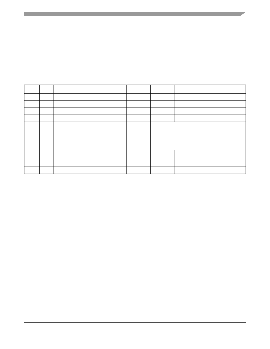
Table A-16. FLASH Characteristics
Num
C
Characteristic
Symbol
Min
Typical
Max
Unit
1
—
Supply voltage for program/erase
Vprog/erase
2.7
5.5
V
2
—
Supply voltage for read operation
VRead
2.7
5.5
V
3
—
Internal FCLK frequency1
1
The frequency of this clock is controlled by a software setting.
fFCLK
150
200
kHz
4
—
Internal FCLK period (1/fFCLK)tFcyc
5
6.67
μs
5
—
Byte program time (random location)2
2 These values are hardware state machine controlled. User code does not need to count cycles. This information supplied for
calculating approximate time to program and erase.
tprog
9tFcyc
6
—
Byte program time (burst mode)2
tBurst
4tFcyc
7
—
Page erase time2
tPage
4000
tFcyc
8
—
Mass erase time2
tMass
20,000
tFcyc
9C
Program/erase endurance3
TL to TH = –40°C to +125°C
T = 25
°C
3 Typical endurance for FLASH is based on the intrinsic bit cell performance. For additional information on how Freescale
denes typical endurance, please refer to Engineering Bulletin EB619/D, Typical Endurance for Nonvolatile Memory.
nFLPE
10,000
—
100,000
—
cycles
10
C
Data retention4
4 Typical data retention values are based on intrinsic capability of the technology measured at high temperature and de-rated
to 25
°C using the Arrhenius equation. For additional information on how Freescale denes typical data retention, please refer
to Engineering Bulletin EB618/D, Typical Data Retention for Nonvolatile Memory.
tD_ret
15
100
—
years
相關(guān)PDF資料 |
PDF描述 |
|---|---|
| MC9S08SH4CTGR | MICROCONTROLLER, PDSO16 |
| MC9S08SH4MSCR | MICROCONTROLLER, PDSO8 |
| MC9S08SH8MTG | MICROCONTROLLER, PDSO16 |
| MC9S08SH8CTGR | MICROCONTROLLER, PDSO16 |
| MC9S08SH8MTJR | MICROCONTROLLER, PDSO20 |
相關(guān)代理商/技術(shù)參數(shù) |
參數(shù)描述 |
|---|---|
| MC9S08SG8 | 制造商:FREESCALE 制造商全稱:Freescale Semiconductor, Inc 功能描述:Microcontrollers |
| MC9S08SG8_09 | 制造商:FREESCALE 制造商全稱:Freescale Semiconductor, Inc 功能描述:Microcontrollers |
| MC9S08SG8_12 | 制造商:FREESCALE 制造商全稱:Freescale Semiconductor, Inc 功能描述:MC9S08SG8 |
| MC9S08SG8CXXE | 制造商:FREESCALE 制造商全稱:Freescale Semiconductor, Inc 功能描述:Microcontrollers |
| MC9S08SG8MXXE | 制造商:FREESCALE 制造商全稱:Freescale Semiconductor, Inc 功能描述:Microcontrollers |
發(fā)布緊急采購,3分鐘左右您將得到回復(fù)。