- 您現(xiàn)在的位置:買賣IC網(wǎng) > PDF目錄371065 > MC74HC4316D (MOTOROLA INC) Single Timer; Package: DIP; No of Pins: 8; Container: Rail PDF資料下載
參數(shù)資料
| 型號(hào): | MC74HC4316D |
| 廠商: | MOTOROLA INC |
| 元件分類: | 運(yùn)動(dòng)控制電子 |
| 英文描述: | Single Timer; Package: DIP; No of Pins: 8; Container: Rail |
| 中文描述: | QUAD 1-CHANNEL, SGL POLE SGL THROW SWITCH, PDSO16 |
| 封裝: | PLASTIC, SOIC-16 |
| 文件頁(yè)數(shù): | 1/10頁(yè) |
| 文件大?。?/td> | 347K |
| 代理商: | MC74HC4316D |
SEMICONDUCTOR TECHNICAL DATA
1
REV 6
Motorola, Inc. 1995
10/95
# $"
#"% #"% $"
" "
$ #!
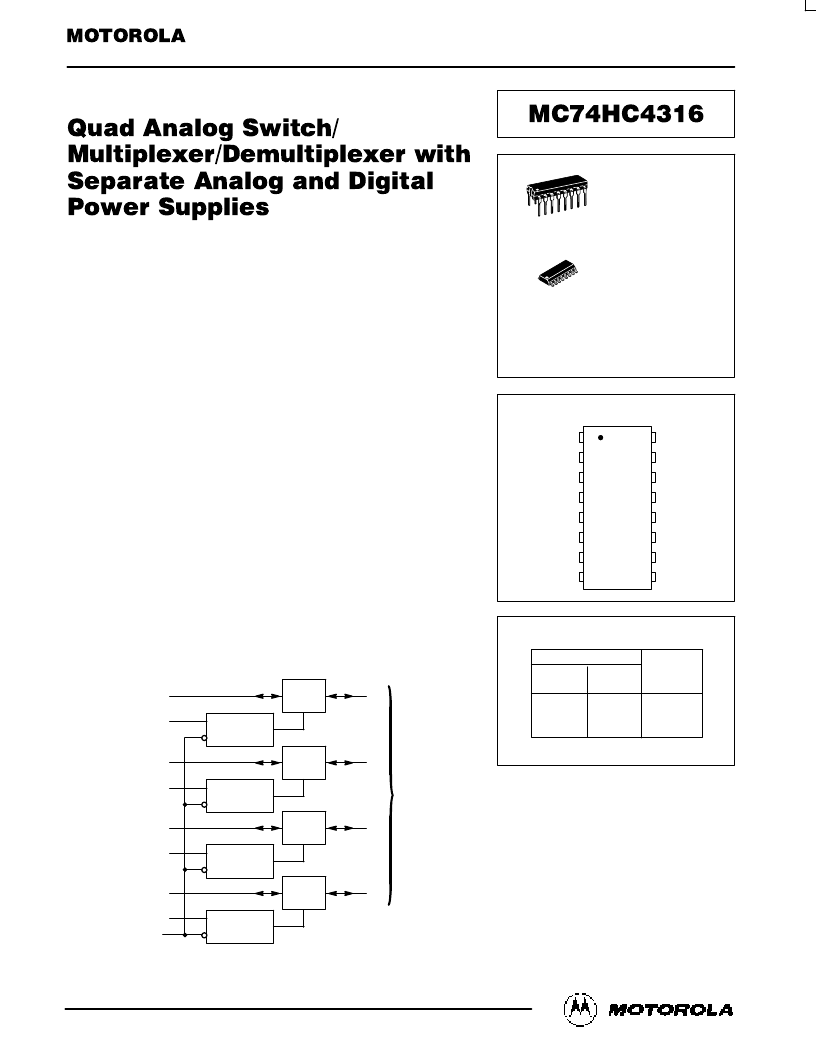
High–Performance Silicon–Gate CMOS
The MC74HC4316 utilizes silicon–gate CMOS technology to achieve fast
propagation delays, low ON resistances, and low OFF–channel leakage
current. This bilateral switch/multiplexer/demultiplexer controls analog and
digital voltages that may vary across the full analog power–supply range
(from VCC to VEE).
The HC4316 is similar in function to the metal–gate CMOS MC14016 and
MC14066, and to the High–Speed CMOS HC4016 and HC4066. Each
device has four independent switches. The device control and Enable inputs
are compatible with standard CMOS outputs; with pullup resistors, they are
compatible with LSTTL outputs. The device has been designed so that the
ON resistances (RON) are much more linear over input voltage than RON of
metal–gate CMOS analog switches. Logic–level translators are provided so
that the On/Off Control and Enable logic–level voltages need only be VCC
and GND, while the switch is passing signals ranging between VCC and VEE.
When the Enable pin (active–low) is high, all four analog switches are turned
off.
Logic–Level Translator for On/Off Control and Enable Inputs
Fast Switching and Propagation Speeds
High ON/OFF Output Voltage Ratio
Diode Protection on All Inputs/Outputs
Analog Power–Supply Voltage Range (VCC – VEE) = 2.0 to 12.0 Volts
Digital (Control) Power–Supply Voltage Range (VCC – GND) = 2.0 to
6.0 Volts, Independent of VEE
Improved Linearity of ON Resistance
Chip Complexity: 66 FETs or 16.5 Equivalent Gates
LOGIC DIAGRAM
XA
A ON/OFF CONTROL
ANALOG
SWITCH
LEVEL
TRANSLATOR
ANALOG
OUTPUTS/INPUTS
PIN 16 = VCC
PIN 8 = GND
PIN 9 = VEE
GND
≥
VEE
2
YA
1
15
XB
B ON/OFF CONTROL
ANALOG
SWITCH
LEVEL
TRANSLATOR
3
YB
4
5
XC
C ON/OFF CONTROL
ANALOG
SWITCH
LEVEL
TRANSLATOR
11
YC
10
6
XD
D ON/OFF CONTROL
ENABLE
ANALOG
SWITCH
LEVEL
TRANSLATOR
12
YD
13
14
7
ANALOG INPUTS/OUTPUTS = XA, XB, XC, XD
FUNCTION TABLE
Inputs
On/Off
Enable
Control
L
L
H
PIN ASSIGNMENT
13
14
15
16
9
10
11
12
5
4
3
2
1
8
7
6
YD
XD
D ON/OFF
CONTROL
A ON/OFF
CONTROL
VCC
VEE
XC
YC
XB
YB
YA
XA
GND
ENABLE
C ON/OFF
CONTROL
B ON/OFF
CONTROL
State of
Analog
Switch
On
Off
Off
H
L
X
X = don’t care
D SUFFIX
SOIC PACKAGE
CASE 751B–05
N SUFFIX
PLASTIC PACKAGE
CASE 648–08
1
16
1
16
ORDERING INFORMATION
MC74HCXXXXN
MC74HCXXXXD
Plastic
SOIC
相關(guān)PDF資料 |
PDF描述 |
|---|---|
| MC74HC4316N | Dual Timer; Package: SOP; No of Pins: 14; Container: Rail |
| MC74HC4353DW | Analog Multiplexers/Demultiplexers with Address Latch |
| MC74HC4353 | Analog Multiplexers/Demultiplexers with Address Latch |
| MC74HC4353N | Analog Multiplexers/Demultiplexers with Address Latch |
| MC54HC4353J | Analog Multiplexers/Demultiplexers with Address Latch |
相關(guān)代理商/技術(shù)參數(shù) |
參數(shù)描述 |
|---|---|
| MC74HC4316DR2 | 制造商:ON Semiconductor 功能描述:Analog Switch Quad SPST 16-Pin SOIC T/R |
| MC74HC4316F | 制造商:Rochester Electronics LLC 功能描述:- Bulk |
| MC74HC4316FEL | 制造商:Rochester Electronics LLC 功能描述:- Bulk |
| MC74HC4316FL1 | 制造商:Rochester Electronics LLC 功能描述:- Bulk |
| MC74HC4316FR1 | 制造商:Rochester Electronics LLC 功能描述:- Bulk |
發(fā)布緊急采購(gòu),3分鐘左右您將得到回復(fù)。