- 您現(xiàn)在的位置:買賣IC網(wǎng) > PDF目錄382310 > MC74HC4046AN (ON SEMICONDUCTOR) Phase-Locked Loop PDF資料下載
參數(shù)資料
| 型號(hào): | MC74HC4046AN |
| 廠商: | ON SEMICONDUCTOR |
| 元件分類: | XO, clock |
| 英文描述: | Phase-Locked Loop |
| 中文描述: | PHASE LOCKED LOOP, PDIP16 |
| 封裝: | PLASTIC, DIP-16 |
| 文件頁(yè)數(shù): | 1/16頁(yè) |
| 文件大小: | 290K |
| 代理商: | MC74HC4046AN |
當(dāng)前第1頁(yè)第2頁(yè)第3頁(yè)第4頁(yè)第5頁(yè)第6頁(yè)第7頁(yè)第8頁(yè)第9頁(yè)第10頁(yè)第11頁(yè)第12頁(yè)第13頁(yè)第14頁(yè)第15頁(yè)第16頁(yè)

Semiconductor Components Industries, LLC, 2000
March, 2000 – Rev. 7
1
Publication Order Number:
MC74HC4046A/D
High–Performance Silicon–Gate CMOS
The MC74HC4046A is similar in function to the MC14046 Metal
gate CMOS device. The device inputs are compatible with standard
CMOS outputs; with pullup resistors, they are compatible with
LSTTL outputs.
The HC4046A phase–locked loop contains three phase
comparators, a voltage–controlled oscillator (VCO) and unity gain
op–amp DEMOUT. The comparators have two common signal inputs,
COMPIN, and SIGIN. Input SIGIN and COMPIN can be used directly
coupled to large voltage signals, or indirectly coupled (with a series
capacitor to small voltage signals). The self–bias circuit adjusts small
voltage signals in the linear region of the amplifier. Phase comparator
1 (an exclusive OR gate) provides a digital error signal PC1OUT and
maintains 90 degrees phase shift at the center frequency between
SIGIN and COMPIN signals (both at 50% duty cycle). Phase
comparator 2 (with leading–edge sensing logic) provides digital error
signals PC2OUT and PCPOUT and maintains a 0 degree phase shift
between SIGIN and COMPIN signals (duty cycle is immaterial). The
linear VCO produces an output signal VCOOUT whose frequency is
determined by the voltage of input VCOIN signal and the capacitor
and resistors connected to pins C1A, C1B, R1 and R2. The unity gain
op–amp output DEMOUT with an external resistor is used where the
VCOIN signal is needed but no loading can be tolerated. The inhibit
input, when high, disables the VCO and all op–amps to minimize
standby power consumption.
Applications include FM and FSK modulation and demodulation,
frequency synthesis and multiplication, frequency discrimination,
tone decoding, data synchronization and conditioning,
voltage–to–frequency conversion and motor speed control.
Output Drive Capability: 10 LSTTL Loads
Low Power Consumption Characteristic of CMOS Devices
Operating Speeds Similar to LSTTL
Wide Operating Voltage Range: 3.0 to 6.0 V
Low Input Current: 1.0
μ
A Maximum (except SIGIN and COMPIN)
In Compliance with the Requirements Defined by JEDEC Standard
No. 7A
Low Quiescent Current: 80
μ
A Maximum (VCO disabled)
High Noise Immunity Characteristic of CMOS Devices
Diode Protection on all Inputs
Chip Complexity: 279 FETs or 70 Equivalent Gates
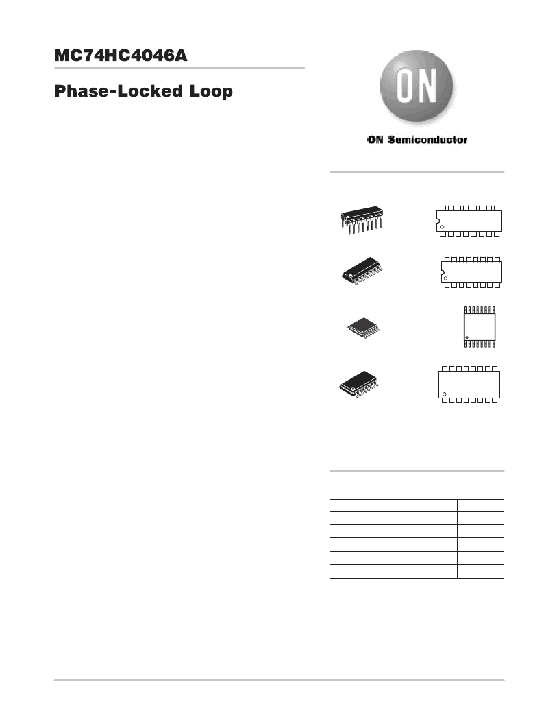
SO–16
D SUFFIX
CASE 751B
http://onsemi.com
1
16
PDIP–16
N SUFFIX
CASE 648
1
16
MARKING
DIAGRAMS
16
1
16
MC74HC4046AN
AWLYYWW
1
HC4046A
AWLYWW
A
WL = Wafer Lot
YY
= Year
WW = Work Week
= Assembly Location
Device
Package
Shipping
ORDERING INFORMATION
MC74HC4046AN
PDIP–16
2000 / Box
MC74HC4046AD
SOIC–16
48 / Rail
MC74HC4046ADR2
SOIC–16
2500 / Reel
TSSOP–16
DT SUFFIX
CASE 948F
1
16
HC40
46A
ALYW
1
16
SOEIAJ–16
F SUFFIX
CASE 966
1
16
74HC4046B
AWLYWW
1
16
MC74HC4046AF
SOIC–EIAJ
See Note
NO TAG
MC74HC4046AFEL
SOIC–EIAJ
1. For ordering information on the EIAJ veNO TAG
SOIC packages, please contact your local ON
Semiconductor representative.
相關(guān)PDF資料 |
PDF描述 |
|---|---|
| MC74HC4538A | Dual Precision Monostable Multivibrator(Retriggerable, Resettable) |
| MC74HC4538 | Dual Precision Monostable Multivibrator(Retriggerable, Resettable) |
| MC74HC4538AD | Dual Precision Monostable Multivibrator(Retriggerable, Resettable) |
| MC74HC4538ADR2 | Dual Precision Monostable Multivibrator(Retriggerable, Resettable) |
| MC74HC4538AN | Dual Precision Monostable Multivibrator(Retriggerable, Resettable) |
相關(guān)代理商/技術(shù)參數(shù) |
參數(shù)描述 |
|---|---|
| MC74HC4046AND | 制造商:Motorola Inc 功能描述: |
| MC74HC4046ANG | 功能描述:鎖相環(huán) - PLL LOG CMOS PLL RoHS:否 制造商:Silicon Labs 類型:PLL Clock Multiplier 電路數(shù)量:1 最大輸入頻率:710 MHz 最小輸入頻率:0.002 MHz 輸出頻率范圍:0.002 MHz to 808 MHz 電源電壓-最大:3.63 V 電源電壓-最小:1.71 V 最大工作溫度:+ 85 C 最小工作溫度:- 40 C 封裝 / 箱體:QFN-36 封裝:Tray |
| MC74HC4049D | 制造商:Rochester Electronics LLC 功能描述:- Bulk |
| MC74HC4049DR2 | 制造商:Rochester Electronics LLC 功能描述:- Bulk |
| MC74HC4049F | 制造商:Rochester Electronics LLC 功能描述:- Bulk |
發(fā)布緊急采購(gòu),3分鐘左右您將得到回復(fù)。