- 您現(xiàn)在的位置:買賣IC網(wǎng) > PDF目錄383563 > MC74ACT273NG (ON SEMICONDUCTOR) Octal D Flip−Flop PDF資料下載
參數(shù)資料
| 型號: | MC74ACT273NG |
| 廠商: | ON SEMICONDUCTOR |
| 元件分類: | 通用總線功能 |
| 英文描述: | Octal D Flip−Flop |
| 中文描述: | ACT SERIES, POSITIVE EDGE TRIGGERED D FLIP-FLOP, TRUE OUTPUT, PDIP20 |
| 封裝: | LEAD FREE, PLASTIC, DIP-20 |
| 文件頁數(shù): | 2/8頁 |
| 文件大?。?/td> | 120K |
| 代理商: | MC74ACT273NG |
MC74AC273, MC74ACT273
http://onsemi.com
2
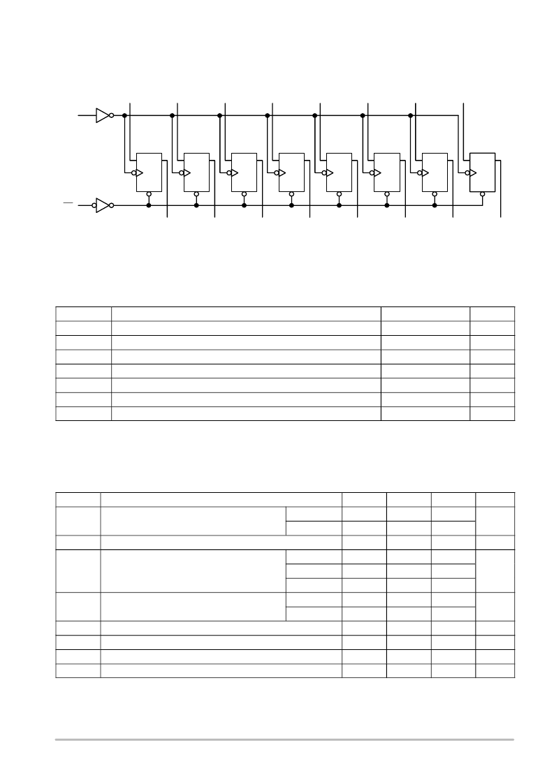
Figure 1. Logic Diagram
D
0
D
1
D
2
D
3
D
4
D
5
D
6
D
7
O
0
O
1
O
2
O
3
O
4
O
5
O
6
O
7
D
Q
CP
R
D
D
Q
CP
R
D
D
Q
CP
R
D
D
Q
CP
R
D
D
Q
CP
R
D
D
Q
CP
R
D
D
Q
CP
R
D
D
Q
CP
R
D
CP
MR
NOTE: That this diagram is provided only for the understanding of logic operations and should not be used to estimate propagation delays.
MAXIMUM RATINGS
Symbol
Parameter
Value
Unit
V
CC
DC Supply Voltage (Referenced to GND)
0.5 to + 7.0
V
V
IN
DC Input Voltage (Referenced to GND)
0.5 to V
CC
+ 0.5
V
V
OUT
DC Output Voltage (Referenced to GND)
0.5 to V
CC
+ 0.5
V
I
IN
DC Input Current, per Pin
±
20
mA
I
OUT
DC Output Sink/Source Current, per Pin
±
50
mA
I
CC
DC V
CC
or GND Current per Output Pin
±
50
mA
T
stg
Storage Temperature
65 to + 150
°
C
Maximum ratings are those values beyond which device damage can occur. Maximum ratings applied to the device are individual stress limit
values (not normal operating conditions) and are not valid simultaneously. If these limits are exceeded, device functional operation is not implied,
damage may occur and reliability may be affected.
RECOMMENDED OPERATING CONDITIONS
Symbol
Parameter
Min
Typ
Max
Unit
V
CC
Supply Voltage
′
AC
2.0
5.0
6.0
V
′
ACT
4.5
5.0
5.5
V
in
, V
out
DC Input Voltage, Output Voltage (Ref. to GND)
0
V
CC
V
t
r
, t
f
Input Rise and Fall Time (Note 1)
′
AC Devices except Schmitt Inputs
V
CC
@ 3.0 V
150
V
CC
@ 4.5 V
40
ns/V
V
CC
@ 5.5 V
25
t
r
, t
f
Input Rise and Fall Time (Note 2)
′
ACT Devices except Schmitt Inputs
V
CC
@ 4.5 V
10
ns/V
V
CC
@ 5.5 V
8.0
T
J
Junction Temperature (PDIP)
140
°
C
T
A
Operating Ambient Temperature Range
40
25
85
°
C
I
OH
Output Current High
24
mA
I
OL
Output Current Low
24
mA
1. V
IN
from 30% to 70% V
CC
; see individual Data Sheets for devices that differ from the typical input rise and fall times.
2. V
IN
from 0.8 V to 2.0 V; see individual Data Sheets for devices that differ from the typical input rise and fall times.
相關(guān)PDF資料 |
PDF描述 |
|---|---|
| MC74AC273DTR2G | Octal D Flip−Flop |
| MC74AC273DWG | Octal D Flip−Flop |
| MC74AC273DWR2G | Octal D Flip−Flop |
| MC74AC273MELG | Octal D Flip−Flop |
| MC74AC299DW | 8−Input Universal Shift/Storage Register with Common Parallel I/O Pins |
相關(guān)代理商/技術(shù)參數(shù) |
參數(shù)描述 |
|---|---|
| MC74ACT299 | 制造商:ONSEMI 制造商全稱:ON Semiconductor 功能描述:8-Input Universal Shift/ Storage Register with Common Parallel I/O Pins |
| MC74ACT299DW | 功能描述:計數(shù)器移位寄存器 4.5-5.5V 8-Input RoHS:否 制造商:Texas Instruments 計數(shù)器類型: 計數(shù)順序:Serial to Serial/Parallel 電路數(shù)量:1 封裝 / 箱體:SOIC-20 Wide 邏輯系列: 邏輯類型: 輸入線路數(shù)量:1 輸出類型:Open Drain 傳播延遲時間:650 ns 最大工作溫度:+ 125 C 最小工作溫度:- 40 C 封裝:Reel |
| MC74ACT299DWG | 功能描述:計數(shù)器移位寄存器 4.5-5.5V 8-Input Universal Shift RoHS:否 制造商:Texas Instruments 計數(shù)器類型: 計數(shù)順序:Serial to Serial/Parallel 電路數(shù)量:1 封裝 / 箱體:SOIC-20 Wide 邏輯系列: 邏輯類型: 輸入線路數(shù)量:1 輸出類型:Open Drain 傳播延遲時間:650 ns 最大工作溫度:+ 125 C 最小工作溫度:- 40 C 封裝:Reel |
| MC74ACT299DWR2 | 功能描述:計數(shù)器移位寄存器 4.5-5.5V 8-Input RoHS:否 制造商:Texas Instruments 計數(shù)器類型: 計數(shù)順序:Serial to Serial/Parallel 電路數(shù)量:1 封裝 / 箱體:SOIC-20 Wide 邏輯系列: 邏輯類型: 輸入線路數(shù)量:1 輸出類型:Open Drain 傳播延遲時間:650 ns 最大工作溫度:+ 125 C 最小工作溫度:- 40 C 封裝:Reel |
| MC74ACT299DWR2G | 功能描述:計數(shù)器移位寄存器 4.5-5.5V 8-Input Universal Shift RoHS:否 制造商:Texas Instruments 計數(shù)器類型: 計數(shù)順序:Serial to Serial/Parallel 電路數(shù)量:1 封裝 / 箱體:SOIC-20 Wide 邏輯系列: 邏輯類型: 輸入線路數(shù)量:1 輸出類型:Open Drain 傳播延遲時間:650 ns 最大工作溫度:+ 125 C 最小工作溫度:- 40 C 封裝:Reel |
發(fā)布緊急采購,3分鐘左右您將得到回復(fù)。