- 您現(xiàn)在的位置:買賣IC網 > PDF目錄383563 > MC74AC273NG (ON SEMICONDUCTOR) Octal D Flip−Flop PDF資料下載
參數(shù)資料
| 型號: | MC74AC273NG |
| 廠商: | ON SEMICONDUCTOR |
| 元件分類: | 通用總線功能 |
| 英文描述: | Octal D Flip−Flop |
| 中文描述: | AC SERIES, POSITIVE EDGE TRIGGERED D FLIP-FLOP, TRUE OUTPUT, PDIP20 |
| 封裝: | LEAD FREE, PLASTIC, DIP-20 |
| 文件頁數(shù): | 4/8頁 |
| 文件大小: | 120K |
| 代理商: | MC74AC273NG |
MC74AC273, MC74ACT273
http://onsemi.com
4
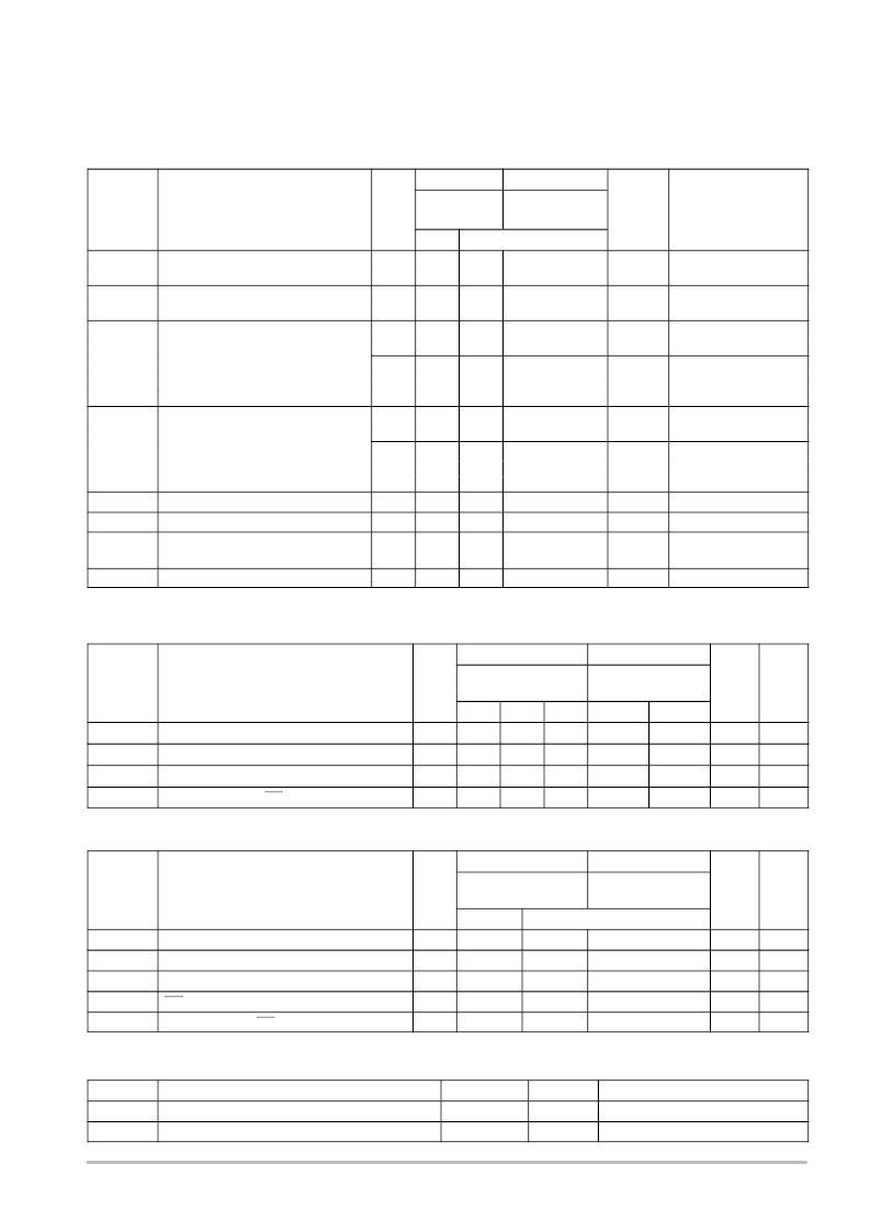
DC CHARACTERISTICS
Symbol
Parameter
V
CC
(V)
74ACT
74ACT
Unit
Conditions
T
A
= +25
°
C
T
A
=
40
°
C to +85
°
C
Typ
Guaranteed Limits
V
IH
Minimum High Level Input Voltage
4.5
5.5
1.5
1.5
2.0
2.0
2.0
2.0
V
V
OUT
= 0.1 V
or V
CC
0.1 V
V
OUT
= 0.1 V
or V
CC
0.1 V
I
OUT
= 50 A
V
IL
Maximum Low Level Input Voltage
4.5
5.5
1.5
1.5
0.8
0.8
0.8
0.8
V
V
OH
Minimum High Level Output Voltage
4.5
5.5
4.49
5.49
4.4
5.4
4.4
5.4
V
*V
IN
= V
IL
or V
IH
I
OH
24 mA
24 mA
4.5
5.5
3.86
4.86
3.76
4.76
V
V
OL
Maximum Low Level Output Voltage
4.5
5.5
0.001
0.001
0.1
0.1
0.1
0.1
V
I
OUT
= 50 A
*V
IN
= V
IL
or V
IH
24 mA
24 mA
4.5
5.5
0.36
0.36
±
0.1
0.44
0.44
±
1.0
1.5
V
I
OL
I
IN
I
CCT
I
OLD
I
OHD
Maximum Input Leakage Current
5.5
A
V
I
= V
CC
, GND
V
I
= V
CC
2.1 V
V
OLD
= 1.65 V Max
V
OHD
= 3.85 V Min
Additional Max. I
CC
/Input
Minimum Dynamic Output Current
5.5
0.6
mA
5.5
5.5
75
75
mA
I
CC
Maximum Quiescent Supply Current
*All outputs loaded; thresholds on input associated with output under test.
Maximum test duration 2.0 ms, one output loaded at a time.
5.5
8.0
80
A
V
IN
= V
CC
or GND
AC CHARACTERISTICS
(For Figures and Waveforms See Section 3 of the ON Semiconductor FACT Data Book, DL138/D)
Symbol
Parameter
V
CC
*
(V)
74ACT
74ACT
Unit
Figure
No.
T
A
= +25
°
C C
L
= 50 pF
T
A
= 40
°
C to +85
°
C
C
L
= 50 pF
Min
Typ
Max
Min
Max
f
max
t
PHL
Maximum Clock Frequency
5.0
125
200
125
MHz
33
Propagation Delay Clock to Output
5.0
3.0
6.0
10
2.5
11.0
ns
36
t
PLH
Propagation Delay Clock to Output
5.0
3.0
6.5
11
2.5
12.0
ns
36
t
PHL
Propagation Delay MR to Output
*Voltage Range 5.0 V is 5.0 V
±
0.5 V.
5.0
3.0
7.0
11
2.5
11.5
ns
36
AC OPERATING REQUIREMENTS
Symbol
Parameter
V
CC
*
(V)
74ACT
74ACT
Unit
Figure
No.
T
A
= +25
°
C C
L
= 50 pF
T
A
= 40
°
C to +85
°
C
C
L
= 50 pF
Typ
Guaranteed Minimum
t
s
t
h
t
w
t
w
t
rec
Setup Time, HIGH or LOW Data to CP
5.0
3.0
4.5
5.0
ns
39
Hold Time, HIGH or LOW Data to CP
5.0
2.5
2.0
2.0
ns
39
Clock Pulse Width HIGH or LOW
5.0
2.5
4.0
4.5
ns
36
MR Pulse Width HIGH or LOW
5.0
2.5
4.0
4.5
ns
36
Recovery Time MR to CP
5.0
1.0
2.0
3.0
ns
36
*Voltage Range 5.0 V is 5.0 V
±
0.5 V.
CAPACITANCE
Symbol
Parameter
Value Typ
Unit
Test Conditions
C
IN
C
PD
Input Capacitance
4.5
pF
V
CC
= 5.0 V
V
CC
= 5.0 V
Power Dissipation Capacitance
50
pF
相關PDF資料 |
PDF描述 |
|---|---|
| MC74ACT273DTR2G | Octal D Flip−Flop |
| MC74ACT273DWG | Octal D Flip−Flop |
| MC74ACT273DWR2G | Octal D Flip−Flop |
| MC74ACT273MELG | Octal D Flip−Flop |
| MC74ACT273MG | Octal D Flip−Flop |
相關代理商/技術參數(shù) |
參數(shù)描述 |
|---|---|
| MC74AC299 | 制造商:ONSEMI 制造商全稱:ON Semiconductor 功能描述:8-Input Universal Shift/ Storage Register with Common Parallel I/O Pins |
| MC74AC299DW | 制造商:ONSEMI 制造商全稱:ON Semiconductor 功能描述:8-Input Universal Shift/ Storage Register with Common Parallel I/O Pins |
| MC74AC299DWR2 | 制造商:ONSEMI 制造商全稱:ON Semiconductor 功能描述:8-Input Universal Shift/ Storage Register with Common Parallel I/O Pins |
| MC74AC299N | 制造商:ONSEMI 制造商全稱:ON Semiconductor 功能描述:8-Input Universal Shift/ Storage Register with Common Parallel I/O Pins |
| MC74AC32 | 制造商:ONSEMI 制造商全稱:ON Semiconductor 功能描述:QUAD 2-INPUT OR GATE |
發(fā)布緊急采購,3分鐘左右您將得到回復。