- 您現(xiàn)在的位置:買賣IC網(wǎng) > PDF目錄45249 > MC7448VS1700LD (FREESCALE SEMICONDUCTOR INC) 32-BIT, 1700 MHz, RISC PROCESSOR, CBGA360 PDF資料下載
參數(shù)資料
| 型號(hào): | MC7448VS1700LD |
| 廠商: | FREESCALE SEMICONDUCTOR INC |
| 元件分類: | 微控制器/微處理器 |
| 英文描述: | 32-BIT, 1700 MHz, RISC PROCESSOR, CBGA360 |
| 封裝: | 25 X 25 MM, 1.80 MM HEIGHT, 1.27 MM PITCH, ROHS COMPLIANT, HCTE, CERAMIC, LGA-360 |
| 文件頁數(shù): | 14/66頁 |
| 文件大小: | 793K |
| 代理商: | MC7448VS1700LD |
第1頁第2頁第3頁第4頁第5頁第6頁第7頁第8頁第9頁第10頁第11頁第12頁第13頁當(dāng)前第14頁第15頁第16頁第17頁第18頁第19頁第20頁第21頁第22頁第23頁第24頁第25頁第26頁第27頁第28頁第29頁第30頁第31頁第32頁第33頁第34頁第35頁第36頁第37頁第38頁第39頁第40頁第41頁第42頁第43頁第44頁第45頁第46頁第47頁第48頁第49頁第50頁第51頁第52頁第53頁第54頁第55頁第56頁第57頁第58頁第59頁第60頁第61頁第62頁第63頁第64頁第65頁第66頁
MPC7448 RISC Microprocessor Hardware Specifications, Rev. 4
Freescale Semiconductor
21
Electrical and Thermal Characteristics
5.2.3
IEEE Std. 1149.1 AC Timing Specifications
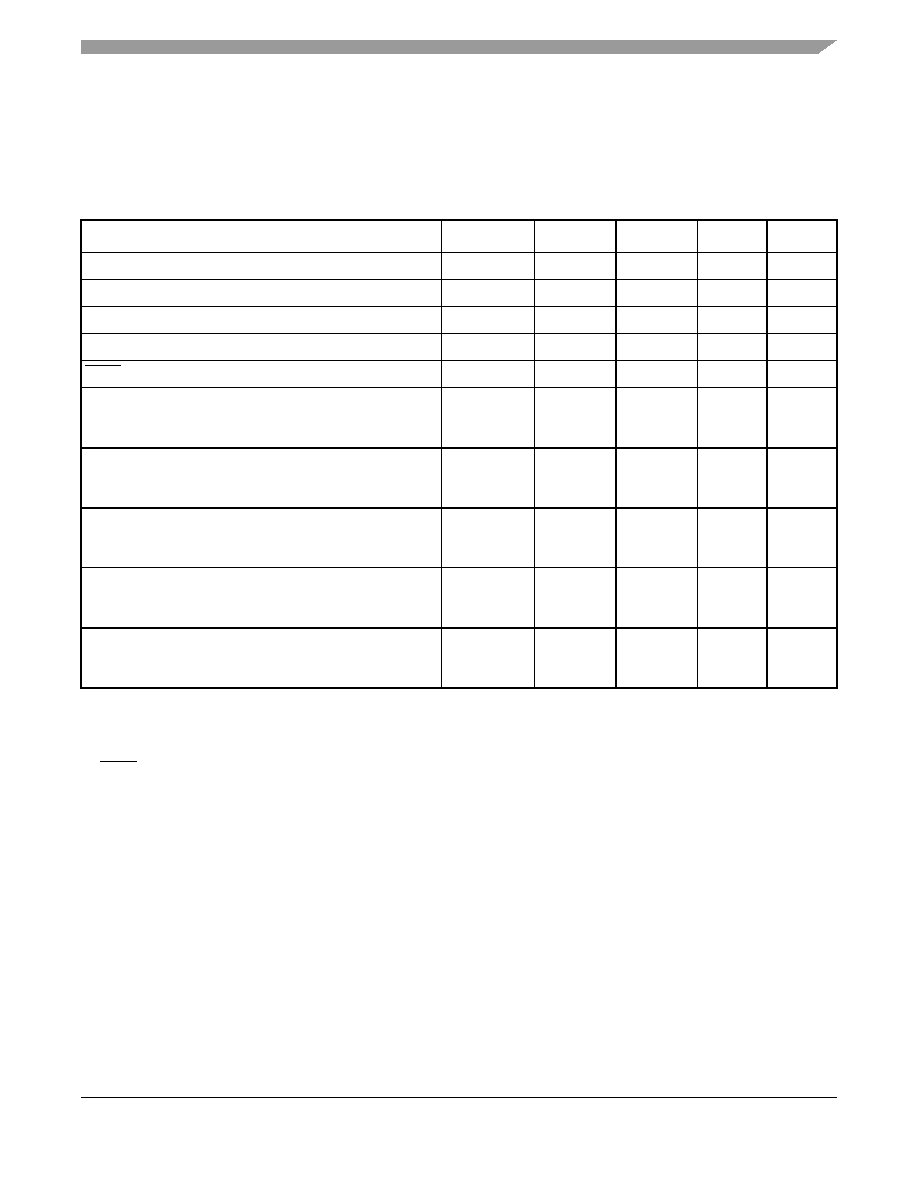
Table 10 provides the IEEE Std. 1149.1 (JTAG) AC timing specifications as defined in Figure 8 through
Table 10. JTAG AC Timing Specifications (Independent of SYSCLK)1
At recommended operating conditions. See Table 4.
Parameter
Symbol
Min
Max
Unit
Notes
TCK frequency of operation
fTCLK
033.3
MHz
TCK cycle time
tTCLK
30
—
ns
TCK clock pulse width measured at 1.4 V
tJHJL
15
—
ns
TCK rise and fall times
tJR and tJF
—2
ns
TRST assert time
tTRST
25
—
ns
2
Input setup times:
Boundary-scan data
TMS, TDI
tDVJH
tIVJH
4
0
—
ns
3
Input hold times:
Boundary-scan data
TMS, TDI
tDXJH
tIXJH
20
25
—
ns
3
Valid times:
Boundary-scan data
TDO
tJLDV
tJLOV
4
20
25
ns
4
Output hold times:
Boundary-scan data
TDO
tJLDX
tJLOX
30
—
ns
4
TCK to output high impedance:
Boundary-scan data
TDO
tJLDZ
tJLOZ
3
19
9
ns
4, 5
Notes:
1. All outputs are measured from the midpoint voltage of the falling/rising edge of TCLK to the midpoint of the signal in question.
The output timings are measured at the pins. All output timings assume a purely resistive 50-
Ω load (see Figure 7).
Time-of-flight delays must be added for trace lengths, vias, and connectors in the system.
2. TRST is an asynchronous level sensitive signal. The time is for test purposes only.
3. Non-JTAG signal input timing with respect to TCK.
4. Non-JTAG signal output timing with respect to TCK.
5. Guaranteed by design and characterization.
相關(guān)PDF資料 |
PDF描述 |
|---|---|
| MC7448VS1600LC | 32-BIT, 1600 MHz, RISC PROCESSOR, CBGA360 |
| MC7448VU1700LD | 32-BIT, 1700 MHz, RISC PROCESSOR, CBGA360 |
| MC7448VU1700LC | 32-BIT, 1700 MHz, RISC PROCESSOR, CBGA360 |
| MC7448HX1600LC | 32-BIT, 1600 MHz, RISC PROCESSOR, CBGA360 |
| MC7448VS1000LD | 32-BIT, 1000 MHz, RISC PROCESSOR, CBGA360 |
相關(guān)代理商/技術(shù)參數(shù) |
參數(shù)描述 |
|---|---|
| MC7448VS600N | 制造商:FREESCALE 制造商全稱:Freescale Semiconductor, Inc 功能描述:MPC7448 Hardware Specifications |
| MC7448VS600NC | 功能描述:IC MPU RISC 600MHZ 360-FCCLGA RoHS:是 類別:集成電路 (IC) >> 嵌入式 - 微處理器 系列:MPC74xx 標(biāo)準(zhǔn)包裝:1 系列:MPC85xx 處理器類型:32-位 MPC85xx PowerQUICC III 特點(diǎn):- 速度:1.2GHz 電壓:1.1V 安裝類型:表面貼裝 封裝/外殼:783-BBGA,F(xiàn)CBGA 供應(yīng)商設(shè)備封裝:783-FCPBGA(29x29) 包裝:托盤 |
| MC7448VS600ND | 功能描述:微處理器 - MPU APL8 RV2.2.1 1.0V 105C RoHS:否 制造商:Atmel 處理器系列:SAMA5D31 核心:ARM Cortex A5 數(shù)據(jù)總線寬度:32 bit 最大時(shí)鐘頻率:536 MHz 程序存儲(chǔ)器大小:32 KB 數(shù)據(jù) RAM 大小:128 KB 接口類型:CAN, Ethernet, LIN, SPI,TWI, UART, USB 工作電源電壓:1.8 V to 3.3 V 最大工作溫度:+ 85 C 安裝風(fēng)格:SMD/SMT 封裝 / 箱體:FBGA-324 |
| MC7448VS667N | 制造商:FREESCALE 制造商全稱:Freescale Semiconductor, Inc 功能描述:MPC7448 Hardware Specifications |
| MC7448VS667NC | 功能描述:IC MPU RISC 667MHZ 360-FCCLGA RoHS:是 類別:集成電路 (IC) >> 嵌入式 - 微處理器 系列:MPC74xx 標(biāo)準(zhǔn)包裝:1 系列:MPC85xx 處理器類型:32-位 MPC85xx PowerQUICC III 特點(diǎn):- 速度:1.2GHz 電壓:1.1V 安裝類型:表面貼裝 封裝/外殼:783-BBGA,F(xiàn)CBGA 供應(yīng)商設(shè)備封裝:783-FCPBGA(29x29) 包裝:托盤 |
發(fā)布緊急采購(gòu),3分鐘左右您將得到回復(fù)。