- 您現(xiàn)在的位置:買賣IC網(wǎng) > PDF目錄371054 > MC68HSC705C8A (Motorola, Inc.) HCMOS Microcontroller Unit PDF資料下載
參數(shù)資料
| 型號: | MC68HSC705C8A |
| 廠商: | Motorola, Inc. |
| 英文描述: | HCMOS Microcontroller Unit |
| 中文描述: | HCMOS微控制器 |
| 文件頁數(shù): | 149/222頁 |
| 文件大小: | 2253K |
| 代理商: | MC68HSC705C8A |
第1頁第2頁第3頁第4頁第5頁第6頁第7頁第8頁第9頁第10頁第11頁第12頁第13頁第14頁第15頁第16頁第17頁第18頁第19頁第20頁第21頁第22頁第23頁第24頁第25頁第26頁第27頁第28頁第29頁第30頁第31頁第32頁第33頁第34頁第35頁第36頁第37頁第38頁第39頁第40頁第41頁第42頁第43頁第44頁第45頁第46頁第47頁第48頁第49頁第50頁第51頁第52頁第53頁第54頁第55頁第56頁第57頁第58頁第59頁第60頁第61頁第62頁第63頁第64頁第65頁第66頁第67頁第68頁第69頁第70頁第71頁第72頁第73頁第74頁第75頁第76頁第77頁第78頁第79頁第80頁第81頁第82頁第83頁第84頁第85頁第86頁第87頁第88頁第89頁第90頁第91頁第92頁第93頁第94頁第95頁第96頁第97頁第98頁第99頁第100頁第101頁第102頁第103頁第104頁第105頁第106頁第107頁第108頁第109頁第110頁第111頁第112頁第113頁第114頁第115頁第116頁第117頁第118頁第119頁第120頁第121頁第122頁第123頁第124頁第125頁第126頁第127頁第128頁第129頁第130頁第131頁第132頁第133頁第134頁第135頁第136頁第137頁第138頁第139頁第140頁第141頁第142頁第143頁第144頁第145頁第146頁第147頁第148頁當(dāng)前第149頁第150頁第151頁第152頁第153頁第154頁第155頁第156頁第157頁第158頁第159頁第160頁第161頁第162頁第163頁第164頁第165頁第166頁第167頁第168頁第169頁第170頁第171頁第172頁第173頁第174頁第175頁第176頁第177頁第178頁第179頁第180頁第181頁第182頁第183頁第184頁第185頁第186頁第187頁第188頁第189頁第190頁第191頁第192頁第193頁第194頁第195頁第196頁第197頁第198頁第199頁第200頁第201頁第202頁第203頁第204頁第205頁第206頁第207頁第208頁第209頁第210頁第211頁第212頁第213頁第214頁第215頁第216頁第217頁第218頁第219頁第220頁第221頁第222頁
Serial Peripheral Interface (SPI)
SPI I/O Registers
MC68HC705C8A
—
Rev. 3
Technical Data
MOTOROLA
Serial Peripheral Interface (SPI)
149
11.9.1 SPI Data Register
The SPDR shown in
Figure 11-7
is the read buffer for characters
received by the SPI. Writing a byte to the SPDR places the byte directly
into the SPI shift register.
11.9.2 SPI Control Register
Enables SPI interrupt requests
Enables the SPI
Configures the SPI as master or slave
Selects serial clock polarity, phase, and frequency
SPIE
—
SPI Interrupt Enable Bit
This read/write bit enables SPI interrupts. Reset clears the SPIE bit.
1 = SPI interrupts enabled
0 = SPI interrupts disabled
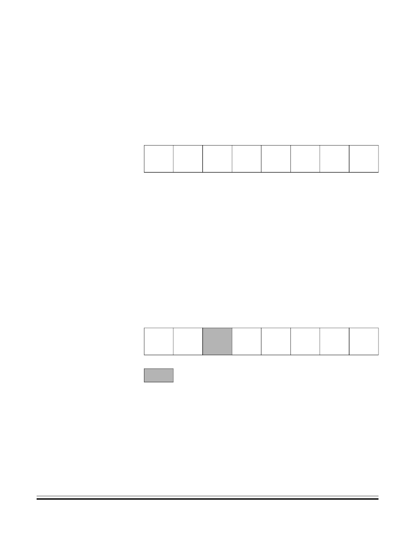
Address:
$000C
Bit 7
6
5
4
3
2
1
Bit 0
Read:
Bit 7
Bit 6
Bit 5
Bit 4
Bit 3
Bit 2
Bit 1
Bit 0
Write:
Reset:
Unaffected by reset
Figure 11-7. SPI Data Register (SPDR)
Address:
$000A
Bit 7
6
5
4
3
2
1
Bit 0
Read:
SPIE
SPE
MSTR
CPOL
CPHA
SPR1
SPR0
Write:
Reset:
0
0
0
U
U
U
U
= Unimplemented
U = Unaffected
Figure 11-8. SPI Control Register (SPCR)
相關(guān)PDF資料 |
PDF描述 |
|---|---|
| MC68HSC705C8ACB | M68HC05 MICROCONTROLLERS |
| MC68HSC705C8ACFB | M68HC05 MICROCONTROLLERS |
| MC68HSC705C8ACFN | M68HC05 MICROCONTROLLERS |
| MC68HSC705C8ACP | M68HC05 MICROCONTROLLERS |
| MC68LC302 | 32-Bit Microprocessor(32位微處理器) |
相關(guān)代理商/技術(shù)參數(shù) |
參數(shù)描述 |
|---|---|
| MC68HSC705C8ACFB | 制造商:Rochester Electronics LLC 功能描述:8 BIT MCU, 304 BYTES RAM - Bulk |
| MC68HSC705C8ACP | 制造商:Rochester Electronics LLC 功能描述: 制造商:Freescale Semiconductor 功能描述: |
| MC68HSC705C8ACS | 制造商:Rochester Electronics LLC 功能描述:- Bulk |
| MC68HSC705J1ACDW | 制造商:Rochester Electronics LLC 功能描述:- Bulk |
| MC68HSC705J1ACP | 制造商:Rochester Electronics LLC 功能描述:8 BIT MCU, 64 BYTES RAM - Bulk |
發(fā)布緊急采購,3分鐘左右您將得到回復(fù)。