- 您現(xiàn)在的位置:買賣IC網(wǎng) > PDF目錄45245 > MC68HLC908QY4CDW (MOTOROLA INC) 8-BIT, FLASH, 2 MHz, MICROCONTROLLER, PDSO16 PDF資料下載
參數(shù)資料
| 型號: | MC68HLC908QY4CDW |
| 廠商: | MOTOROLA INC |
| 元件分類: | 微控制器/微處理器 |
| 英文描述: | 8-BIT, FLASH, 2 MHz, MICROCONTROLLER, PDSO16 |
| 封裝: | SOIC-16 |
| 文件頁數(shù): | 108/186頁 |
| 文件大?。?/td> | 2583K |
| 代理商: | MC68HLC908QY4CDW |
第1頁第2頁第3頁第4頁第5頁第6頁第7頁第8頁第9頁第10頁第11頁第12頁第13頁第14頁第15頁第16頁第17頁第18頁第19頁第20頁第21頁第22頁第23頁第24頁第25頁第26頁第27頁第28頁第29頁第30頁第31頁第32頁第33頁第34頁第35頁第36頁第37頁第38頁第39頁第40頁第41頁第42頁第43頁第44頁第45頁第46頁第47頁第48頁第49頁第50頁第51頁第52頁第53頁第54頁第55頁第56頁第57頁第58頁第59頁第60頁第61頁第62頁第63頁第64頁第65頁第66頁第67頁第68頁第69頁第70頁第71頁第72頁第73頁第74頁第75頁第76頁第77頁第78頁第79頁第80頁第81頁第82頁第83頁第84頁第85頁第86頁第87頁第88頁第89頁第90頁第91頁第92頁第93頁第94頁第95頁第96頁第97頁第98頁第99頁第100頁第101頁第102頁第103頁第104頁第105頁第106頁第107頁當(dāng)前第108頁第109頁第110頁第111頁第112頁第113頁第114頁第115頁第116頁第117頁第118頁第119頁第120頁第121頁第122頁第123頁第124頁第125頁第126頁第127頁第128頁第129頁第130頁第131頁第132頁第133頁第134頁第135頁第136頁第137頁第138頁第139頁第140頁第141頁第142頁第143頁第144頁第145頁第146頁第147頁第148頁第149頁第150頁第151頁第152頁第153頁第154頁第155頁第156頁第157頁第158頁第159頁第160頁第161頁第162頁第163頁第164頁第165頁第166頁第167頁第168頁第169頁第170頁第171頁第172頁第173頁第174頁第175頁第176頁第177頁第178頁第179頁第180頁第181頁第182頁第183頁第184頁第185頁第186頁
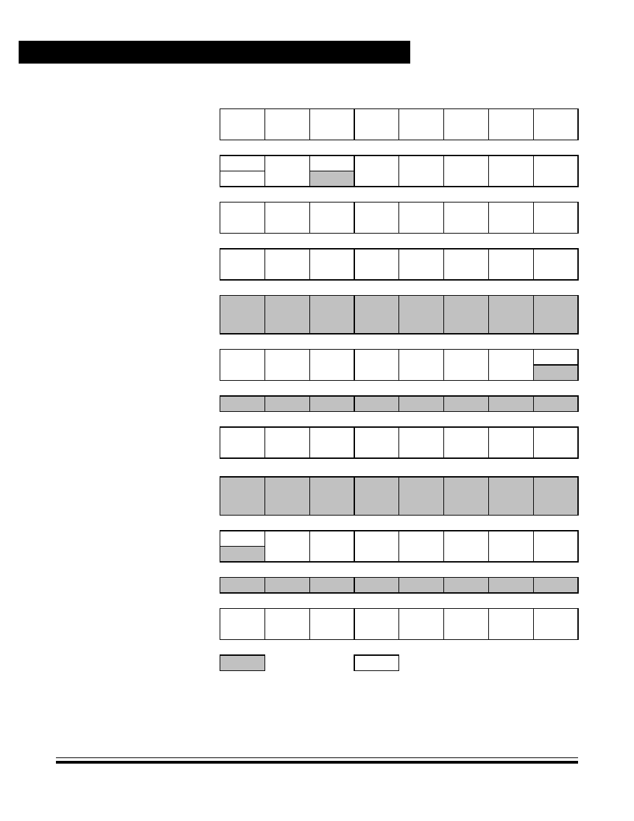
Memory
Data Sheet
MC68HLC908QY/QT Family — Rev. 2
28
Memory
MOTOROLA
$0027
TIM Channel 0
Register Low (TCH0L)
Read:
Bit 7Bit 6Bit 5Bit 4Bit 3Bit 2Bit 1Bit 0
Write:
Reset:
Indeterminate after reset
$0028
TIM Channel 1 Status and
Control Register (TSC1)
Read:
CH1F
CH1IE
0
MS1A
ELS1B
ELS1A
TOV1
CH1MAX
Write:
0
Reset:
00000000
$0029
TIM Channel 1
Register High (TCH1H)
Read:
Bit 15
Bit 14
Bit 13
Bit 12
Bit 11
Bit 10
Bit 9
Bit 8
Write:
Reset:
Indeterminate after reset
$002A
TIM Channel 1
Register Low (TCH1L)
Read:
Bit 7Bit 6Bit 5Bit 4Bit 3Bit 2Bit 1Bit 0
Write:
Reset:
Indeterminate after reset
$002B
↓
$0035
Unimplemented
$0036
Oscillator Status Register
(OSCSTAT)
Read:
RRRRRR
ECGON
ECGST
Write:
Reset:
00000000
$0037
Unimplemented Read:
$0038
Oscillator Trim Register
(OSCTRIM)
Read:
TRIM7
TRIM6
TRIM5
TRIM4
TRIM3
TRIM2
TRIM1
TRIM0
Write:
Reset:
10000000
$0039
↓
$003B
Unimplemented
$003C
ADC Status and Control
Register (ADSCR)
Read:
COCO
AIEN
ADCO
CH4
CH3
CH2
CH1
CH0
Write:
Reset:
00011111
$003D
Unimplemented
$003E
ADC Data Register
(ADR)
Read:
Bit 7Bit 6Bit 5Bit 4Bit 3Bit 2Bit 1Bit 0
Write:
Reset:
Indeterminate after reset
Addr.
Register Name
Bit 7
654321
Bit 0
= Unimplemented
R
= Reserved
U = Unaffected
Figure 2-2. Control, Status, and Data Registers (Sheet 3 of 5)
發(fā)布緊急采購,3分鐘左右您將得到回復(fù)。