- 您現(xiàn)在的位置:買賣IC網(wǎng) > PDF目錄45234 > MC68HC681FN (MOTOROLA INC) 2 CHANNEL(S), 1M bps, SERIAL COMM CONTROLLER, PQCC44 PDF資料下載
參數(shù)資料
| 型號: | MC68HC681FN |
| 廠商: | MOTOROLA INC |
| 元件分類: | 微控制器/微處理器 |
| 英文描述: | 2 CHANNEL(S), 1M bps, SERIAL COMM CONTROLLER, PQCC44 |
| 封裝: | PLASTIC, LCC-44 |
| 文件頁數(shù): | 54/88頁 |
| 文件大?。?/td> | 461K |
| 代理商: | MC68HC681FN |
第1頁第2頁第3頁第4頁第5頁第6頁第7頁第8頁第9頁第10頁第11頁第12頁第13頁第14頁第15頁第16頁第17頁第18頁第19頁第20頁第21頁第22頁第23頁第24頁第25頁第26頁第27頁第28頁第29頁第30頁第31頁第32頁第33頁第34頁第35頁第36頁第37頁第38頁第39頁第40頁第41頁第42頁第43頁第44頁第45頁第46頁第47頁第48頁第49頁第50頁第51頁第52頁第53頁當前第54頁第55頁第56頁第57頁第58頁第59頁第60頁第61頁第62頁第63頁第64頁第65頁第66頁第67頁第68頁第69頁第70頁第71頁第72頁第73頁第74頁第75頁第76頁第77頁第78頁第79頁第80頁第81頁第82頁第83頁第84頁第85頁第86頁第87頁第88頁
Electrical Specifications
5-4
MC68HC681 USER’S MANUAL
MOTOROLA
5
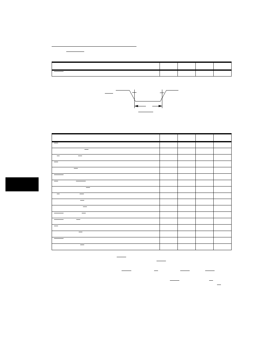
5.5.2 RESET Timing
Figure 5-2. RESET Timing
5.5.3 Read and Write Bus Cycle Timing
CHARACTERISTIC
SYMBOL
MIN
MAX
UNIT
RESET Pulse Width*
tRES
1.0
—
s
NOTE: * The MC68HC681 does not require a clock for correct reset
CHARACTERISTIC
SYMBOL
MIN
MAX
UNIT
CS Setup Time to X1 High 1
tCSC
90
—
ns
RS1-RS4 Setup Time to CS Asserted
tRSS
10
—
ns
R/W Setup Time to CS Asserted
tRWS
10
—
ns
CS Pulse Width Asserted 2
tCSWL
205
—
ns
Data Valid from CS Asserted
tDD
—
175
ns
DTACK Asserted from X1 High
tDCR
—
125
ns
CS Negated from DTACK Asserted 2
tCSD
0—
ns
RS1-RS4 Hold Time from CS Negated
tRSH
0—
ns
R/W Hold Time from CS Negated
tRWH
0—
ns
Data Hold Time from CS Negated
tDH
0—
ns
Data Bus Floating from CS Negated
tDF
—
100
ns
DTACK Negated from CS Negated
tDAH
—
ns
DTACK Hi-Z from CS Negated
tDAT
—
125
ns
CS Pulse Width Negated
tCSWH
90
—
ns
Data Setup Time to CS Negated 3
tDSCS
100
—
ns
DTACK Asserted from X1 High
tDCW
—
125
ns
Data Hold Time from CS Negated
tDH
0—
ns
NOTES:
1.
This specication is only to ensure DTACK is asserted with respect to the rising edge of X1 as shown in Figure 5-3 and Figure 5-
4, not to guarantee operation of the part. If the setup time is violated, DTACKmay be asserted as shown, or may be asserted one
clock cycle later.
2.
This specication is only to ensure that DTACK will be asserted. If CS is negated before DTACK is asserted, DTACK may not be
asserted.
3.
During write cycles, the MC68681 latched data on either the assertion edge of DTACKor the negation edge of CS, whichever
occurred rst. This is not true in the MC68HC681: the MC68HC681 always latches write data on the negation edge of CS.
RESET
tRES
相關PDF資料 |
PDF描述 |
|---|---|
| MC68HC681P | 2 CHANNEL(S), 1M bps, SERIAL COMM CONTROLLER, PDIP40 |
| MC68HC58FN | 1 CHANNEL(S), LOCAL AREA NETWORK CONTROLLER, PQCC28 |
| MC68HC58DW | 1 CHANNEL(S), LOCAL AREA NETWORK CONTROLLER, PDSO28 |
| MC68HC68T1P | 1 TIMER(S), REAL TIME CLOCK, PDIP16 |
| MC68HC705B16NVFNR2 | 8-BIT, OTPROM, 2.1 MHz, MICROCONTROLLER, PQCC52 |
相關代理商/技術參數(shù) |
參數(shù)描述 |
|---|---|
| MC68HC68T1P | 制造商:Motorola Inc 功能描述: |
| MC68HC705B16CFN | 制造商:Motorola Inc 功能描述: |
| MC68HC705B16FN | 制造商:Rochester Electronics LLC 功能描述: |
| MC68HC705B16NB | 制造商:Rochester Electronics LLC 功能描述: |
| MC68HC705B16NCB | 制造商:Rochester Electronics LLC 功能描述: |
發(fā)布緊急采購,3分鐘左右您將得到回復。