- 您現(xiàn)在的位置:買賣IC網(wǎng) > PDF目錄45238 > MC68HC11EA9CFN3 (FREESCALE SEMICONDUCTOR INC) 8-BIT, MROM, 3 MHz, MICROCONTROLLER, PQCC52 PDF資料下載
參數(shù)資料
| 型號: | MC68HC11EA9CFN3 |
| 廠商: | FREESCALE SEMICONDUCTOR INC |
| 元件分類: | 微控制器/微處理器 |
| 英文描述: | 8-BIT, MROM, 3 MHz, MICROCONTROLLER, PQCC52 |
| 封裝: | PLASTIC, LCC-52 |
| 文件頁數(shù): | 9/58頁 |
| 文件大小: | 583K |
| 代理商: | MC68HC11EA9CFN3 |
第1頁第2頁第3頁第4頁第5頁第6頁第7頁第8頁當(dāng)前第9頁第10頁第11頁第12頁第13頁第14頁第15頁第16頁第17頁第18頁第19頁第20頁第21頁第22頁第23頁第24頁第25頁第26頁第27頁第28頁第29頁第30頁第31頁第32頁第33頁第34頁第35頁第36頁第37頁第38頁第39頁第40頁第41頁第42頁第43頁第44頁第45頁第46頁第47頁第48頁第49頁第50頁第51頁第52頁第53頁第54頁第55頁第56頁第57頁第58頁
MC68HC11EA9
MOTOROLA
MC68HC11EA9TS/D
17
5.
Clear the PGM bit to turn off the VPPE voltage.
6.
Clear all bits in the PPROG register to reconfigure the EPROM address and data buses for nor-
mal operation.
NOTE
PROG mode is initiated when RESET, MODA, and MODB pins are pulled low (the
pin state required to enter bootstrap mode). This means that if these three pins are
pulled low and VPPE is present on the XIRQ pin, the EPROM will be programmed.
To prevent this, place a pull-up resistor on the IRQ pin (CE pin in PROG mode).
When the device goes into reset, the PGM bit is forced to the voltage disable state
(EPGM = 0) before the address/data latches are enabled to the external input lines.
Only after this occurs is voltage control returned to the IRQ pin.
4.9.3 Programming EPROM with Downloaded Data
When using this method, the EPROM is programmed by software while in the special test or bootstrap
modes. User-developed software can be uploaded through the SCI, or a ROM resident EPROM pro-
gramming utility can be used. To use the resident utility, bootload a three-byte program consisting of a
single jump instruction to $BF00. $BF00 is the starting address of a resident EPROM programming util-
ity. The utility program sets the X and Y index registers to default values, then receives programming
data from an external host and puts it in EPROM. The value in IX determines programming delay time.
The value in IY is a pointer to the first address in EPROM to be programmed (default = $D000).
When the utility program is ready to receive programming data, it sends the host the $FF character.
Then it waits. When the host sees the $FF character, the EPROM programming data is sent, starting
with the first location in the EPROM array. After the last byte to be programmed is sent and the corre-
sponding verification data is returned, the programming operation is terminated by resetting the MCU.
* MC68HC711EA9 only.
ODD — Program Odd Rows in Half of EEPROM (TEST)
Refer to 4.10 EEPROM.
EVEN — Program Even Rows in Half of EEPROM (TEST)
Refer to 4.10 EEPROM.
ELAT — EPROM/OTPROM Latch Control
When ELAT = 1, writes to EPROM cause address and data to be latched and the EPROM/OTPROM
cannot be read. ELAT can be read any time. ELAT can be written any time except when EPGM = 1;
then the write to ELAT is disabled. For MC68HC711EA9, EPGM enables the high voltage necessary
for both EPROM/OTPROM and EEPROM programming. For MC68HC711EA9 ELAT and EELAT are
mutually exclusive and cannot both equal one.
0 = EPROM address and data bus configured for normal reads
1 = EPROM address and data bus configured for programming
BYTE — Byte/Other EEPROM Erase Mode
Refer to 4.10 EEPROM.
ROW — Row/All EEPROM Erase Mode
Refer to 4.10 EEPROM.
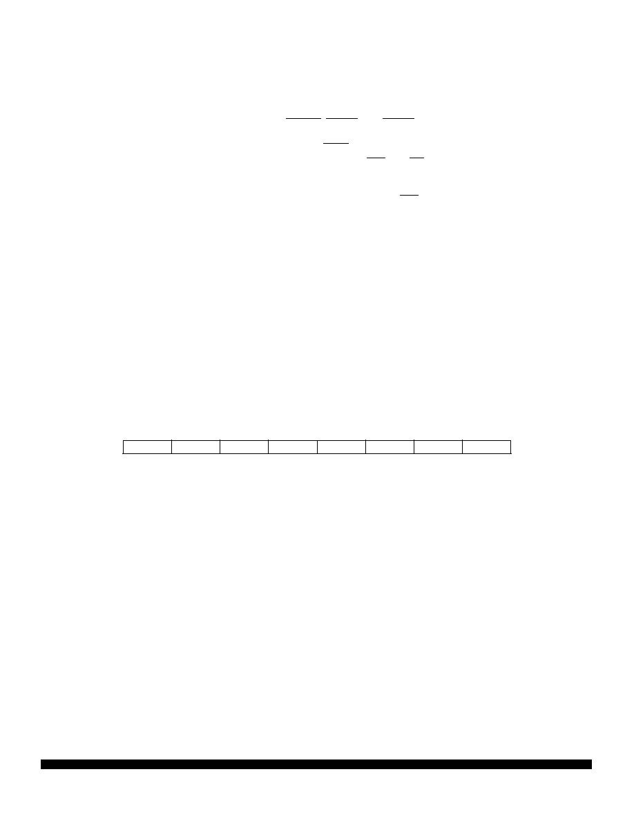
PPROG — EPROM and EEPROM Programming Control Register
$103B
BIT 7
654321
BIT 0
ODD
EVEN
ELAT*
BYTE
ROW
ERASE
EELAT
PGM
RESET:
00000001
F
re
e
sc
a
le
S
e
m
ic
o
n
d
u
c
to
r,
I
Freescale Semiconductor, Inc.
For More Information On This Product,
Go to: www.freescale.com
n
c
..
.
相關(guān)PDF資料 |
PDF描述 |
|---|---|
| MC68HC11EA9MFN2 | 8-BIT, MROM, 2 MHz, MICROCONTROLLER, PQCC52 |
| MC68HC711EA9VP3 | 8-BIT, OTPROM, 3 MHz, MICROCONTROLLER, PDIP56 |
| MC68HC711EA9MFS3 | 8-BIT, UVPROM, 3 MHz, MICROCONTROLLER, CQCC52 |
| MC68HC711EA9MP3 | 8-BIT, OTPROM, 3 MHz, MICROCONTROLLER, PDIP56 |
| MC68HC711EA9VFN3 | 8-BIT, OTPROM, 3 MHz, MICROCONTROLLER, PQCC52 |
相關(guān)代理商/技術(shù)參數(shù) |
參數(shù)描述 |
|---|---|
| MC68HC11EA9CP2 | 制造商:FREESCALE 制造商全稱:Freescale Semiconductor, Inc 功能描述:8-Bit Microcontrollers |
| MC68HC11EA9CP3 | 制造商:FREESCALE 制造商全稱:Freescale Semiconductor, Inc 功能描述:8-Bit Microcontrollers |
| MC68HC11EA9MFN2 | 制造商:FREESCALE 制造商全稱:Freescale Semiconductor, Inc 功能描述:8-Bit Microcontrollers |
| MC68HC11EA9MFN3 | 制造商:FREESCALE 制造商全稱:Freescale Semiconductor, Inc 功能描述:8-Bit Microcontrollers |
| MC68HC11EA9MP2 | 制造商:FREESCALE 制造商全稱:Freescale Semiconductor, Inc 功能描述:8-Bit Microcontrollers |
發(fā)布緊急采購,3分鐘左右您將得到回復(fù)。